Table of Contents
- 1. Product Overview
- 2. In-Depth Technical Parameter Analysis
- 2.1 Absolute Maximum Ratings
- 2.2 Electro-Optical Characteristics
- 3. Binning System Explanation The product is sorted into different performance bins based on radiant intensity measured at IF = 20 mA. This allows for selection consistency in production. The binning is defined as follows: Bin M: Radiant Intensity range from 7.8 mW/sr (Min) to 12.5 mW/sr (Max). Bin N: Radiant Intensity range from 11.0 mW/sr (Min) to 17.6 mW/sr (Max). Bin P: Radiant Intensity range from 15.0 mW/sr (Min) to 24.0 mW/sr (Max). Bin Q: Radiant Intensity range from 21.0 mW/sr (Min) to 34.0 mW/sr (Max). This grading system enables designers to choose components that meet specific minimum output requirements for their application, ensuring system performance. 4. Performance Curve Analysis
- 4.1 Forward Current vs. Ambient Temperature
- 4.2 Spectral Distribution
- 4.3 Radiant Intensity vs. Forward Current
- 4.4 Relative Radiant Intensity vs. Angular Displacement
- 5. Mechanical and Package Information
- 6. Soldering and Assembly Guidelines
- 6.1 Lead Forming
- 6.2 Storage
- 6.3 Soldering Process
- 6.4 Cleaning
- 6.5 Thermal Management
- 7. Packaging and Ordering Information
- 8. Application Recommendations
- 8.1 Typical Application Scenarios
- 8.2 Design Considerations
- 9. Technical Comparison and Differentiation
- 10. Frequently Asked Questions (FAQs)
- 11. Practical Design and Usage Examples
- 12. Operating Principle Introduction
- 13. Technology Trends
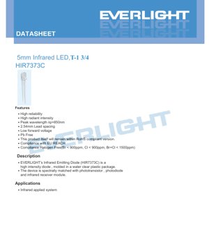
1. Product Overview
This document details the specifications for a high-intensity 5mm infrared (IR) emitting diode. The device is designed for applications requiring reliable infrared emission, featuring a peak wavelength of 850 nanometers (nm). It is housed in a standard T-1 3/4 (5mm) water-clear plastic package, which allows for optimal transmission of the infrared light. The component is spectrally matched with common silicon phototransistors, photodiodes, and infrared receiver modules, making it an ideal source for various IR sensing and communication systems.
The core advantages of this product include high reliability, significant radiant output, and a low forward voltage characteristic, which contributes to energy-efficient operation. It is manufactured to be lead-free (Pb-Free) and complies with major environmental regulations including RoHS, EU REACH, and halogen-free standards (Br < 900ppm, Cl < 900ppm, Br+Cl < 1500ppm). Its primary target market encompasses designers and engineers working on infrared-based systems such as proximity sensors, object detection, remote controls, and industrial automation.
2. In-Depth Technical Parameter Analysis
2.1 Absolute Maximum Ratings
The device is rated for a continuous forward current (IF) of 100 mA. For pulsed operation, it can handle a peak forward current (IFP) of up to 1.0 A under specific conditions: pulse width ≤ 100μs and duty cycle ≤ 1%. The maximum allowable reverse voltage (VR) is 5 V. The operating temperature range is specified from -40°C to +85°C, with a storage temperature range from -40°C to +100°C. The maximum power dissipation (Pd) at or below 25°C free air temperature is 150 mW. The soldering temperature rating is 260°C for a duration not exceeding 5 seconds.
2.2 Electro-Optical Characteristics
Key performance parameters are measured at an ambient temperature (Ta) of 25°C. The radiant intensity (Ie) is the primary optical output metric. At a standard test current of 20 mA, the typical radiant intensity is 15 mW/sr, with a minimum value of 7.8 mW/sr depending on the product bin. At the maximum continuous current of 100 mA (under pulsed conditions), the typical radiant intensity increases to 75 mW/sr.
The peak emission wavelength (λp) is typically 850 nm, with a spectral bandwidth (Δλ) of approximately 45 nm at half maximum intensity. The forward voltage (VF) is typically 1.45 V at 20 mA, with a maximum of 1.65 V. At 100 mA (pulsed), VF ranges from 1.80 V to 2.40 V. The maximum reverse current (IR) is 10 μA when a reverse voltage of 5 V is applied. The viewing angle (2θ1/2), defined as the full angle at half intensity, is typically 40 degrees.
3. Binning System Explanation
The product is sorted into different performance bins based on radiant intensity measured at IF = 20 mA. This allows for selection consistency in production. The binning is defined as follows:
- Bin M: Radiant Intensity range from 7.8 mW/sr (Min) to 12.5 mW/sr (Max).
- Bin N: Radiant Intensity range from 11.0 mW/sr (Min) to 17.6 mW/sr (Max).
- Bin P: Radiant Intensity range from 15.0 mW/sr (Min) to 24.0 mW/sr (Max).
- Bin Q: Radiant Intensity range from 21.0 mW/sr (Min) to 34.0 mW/sr (Max).
This grading system enables designers to choose components that meet specific minimum output requirements for their application, ensuring system performance.
4. Performance Curve Analysis
The datasheet provides several characteristic curves that are crucial for design.
4.1 Forward Current vs. Ambient Temperature
This derating curve shows the maximum allowable continuous forward current as a function of the ambient temperature. As temperature increases, the maximum permissible current decreases linearly to prevent overheating and ensure long-term reliability. Designers must reference this curve to select appropriate operating currents for their expected environmental conditions.
4.2 Spectral Distribution
The spectral distribution graph plots relative radiant intensity against wavelength. It confirms the peak at 850 nm and the approximately 45 nm bandwidth. This curve is important for ensuring compatibility with the spectral sensitivity of the intended receiver (e.g., a phototransistor with peak sensitivity around 850-950 nm).
4.3 Radiant Intensity vs. Forward Current
This graph illustrates the relationship between the drive current and the optical output. The radiant intensity increases super-linearly with current. It helps designers understand the trade-off between drive current, optical power, and device efficiency.
4.4 Relative Radiant Intensity vs. Angular Displacement
This polar plot depicts the emission pattern of the LED. The intensity is highest along the central axis (0°) and decreases as the angle increases, defining the 40-degree viewing angle. This information is vital for optical design, such as lens selection and alignment in sensing applications.
5. Mechanical and Package Information
The device uses a standard 5mm radial leaded package. The package dimension drawing specifies the physical measurements, including the diameter of the epoxy lens (typically 5.0mm), the lead spacing (2.54mm or 0.1 inches, standard for through-hole components), and the overall length. The drawing includes tolerances, typically ±0.25mm for critical dimensions. The anode (positive) lead is typically identified as the longer lead. The water-clear lens material is optimized for infrared transmission with minimal absorption.
6. Soldering and Assembly Guidelines
6.1 Lead Forming
If leads need to be bent, it must be done at a point at least 3mm from the base of the epoxy bulb. Forming should always be performed before soldering and at room temperature to avoid stressing the package or damaging the internal die and wire bonds. The PCB holes must align precisely with the LED leads to prevent mounting stress.
6.2 Storage
Components should be stored in a controlled environment at 30°C or less and 70% relative humidity or less. The recommended storage life after shipment is 3 months. For longer storage (up to one year), they should be kept in a sealed container with a nitrogen atmosphere and desiccant. Rapid temperature changes in humid environments should be avoided to prevent condensation.
6.3 Soldering Process
Soldering must be performed with care to prevent thermal damage. The solder joint should be at least 3mm away from the epoxy bulb.
- Hand Soldering: Maximum iron tip temperature of 300°C (for a 30W iron max), with soldering time not exceeding 3 seconds per lead.
- Wave/Dip Soldering: Maximum preheat temperature of 100°C for up to 60 seconds. The solder bath temperature should not exceed 260°C, with the component immersed for a maximum of 5 seconds.
A recommended soldering temperature profile is provided, emphasizing a controlled ramp-up, peak temperature dwell, and controlled cooldown. Rapid cooling is not recommended. Dip or hand soldering should not be performed more than once. After soldering, the LED should be protected from mechanical shock until it returns to room temperature.
6.4 Cleaning
If cleaning is necessary, use isopropyl alcohol at room temperature for no more than one minute, followed by air drying. Ultrasonic cleaning is generally not recommended due to the risk of damaging the internal structure. If absolutely required, the process must be carefully qualified beforehand.
6.5 Thermal Management
Although this is a low-power device, heat management must be considered in the application design, especially when operating near maximum ratings. The current should be derated according to the Forward Current vs. Ambient Temperature curve to maintain junction temperature within safe limits and ensure long-term reliability.
7. Packaging and Ordering Information
The standard packing specification is as follows: 500 pieces are packed in one anti-static bag. Five of these bags are placed into one inner carton. Ten inner cartons are then packed into one master (outside) carton, resulting in a total of 25,000 pieces per master carton.
The label on the packaging contains several codes: Customer's Product Number (CPN), the manufacturer's Product Number (P/N), Packing Quantity (QTY), Luminous Intensity Rank (CAT), Dominant Wavelength Rank (HUE), Forward Voltage Rank (REF), Lot Number (LOT No.), and a date code (Month X).
8. Application Recommendations
8.1 Typical Application Scenarios
This infrared LED is suitable for a wide range of applications including, but not limited to: Infrared remote control transmitters, proximity and object detection sensors, industrial optical switches and encoders, night vision illumination systems, optical data transmission links, and touchless user interfaces.
8.2 Design Considerations
- Current Limiting: Always use a series current-limiting resistor when driving the LED from a voltage source. The value can be calculated using Ohm's Law: R = (Vsupply - VF) / IF.
- Receiver Matching: Ensure the selected photodetector (phototransistor, photodiode, or IR receiver IC) has peak sensitivity around 850 nm for optimal performance.
- Optical Path: Consider the viewing angle and potential need for lenses or apertures to collimate or focus the IR beam for longer-range or directed applications.
- Electrical Noise: In sensing applications, modulation of the IR signal (e.g., with a specific frequency) and synchronous detection at the receiver can greatly improve immunity to ambient light interference.
9. Technical Comparison and Differentiation
Compared to generic infrared LEDs, this device offers a well-defined combination of high radiant intensity (up to 75 mW/sr typ. at 100mA pulsed) and a relatively low forward voltage (1.45V typ. at 20mA). The 850nm wavelength is a common standard, ensuring broad compatibility with silicon-based receivers. Its compliance with stringent environmental standards (RoHS, REACH, Halogen-Free) makes it suitable for modern electronics requiring green certifications. The clear package provides a consistent, unfiltered output compared to tinted packages that might attenuate the signal.
10. Frequently Asked Questions (FAQs)
Q: What is the difference between radiant intensity (mW/sr) and luminous intensity (mcd)?
A: Radiant intensity measures optical power (in milliwatts) emitted per unit solid angle (steradian), relevant for all wavelengths. Luminous intensity is weighted by the human eye's sensitivity (photopic curve) and is measured in candelas; it is not applicable for infrared sources like this 850nm LED.
Q: Can I drive this LED with a constant current of 100 mA continuously?
A: The Absolute Maximum Rating specifies 100 mA as the maximum continuous forward current. However, for reliable long-term operation, it is advisable to operate below this maximum, especially at higher ambient temperatures, by referring to the derating curve.
Q: Why is the viewing angle specified as 40 degrees?
A> The 40-degree angle (2θ1/2) is the full width at the points where the radiant intensity drops to half of its peak value on the central axis. It describes the beam spread of the LED.
Q: Is an ESD protection diode required for this LED?
A> While the datasheet does not specify a high ESD rating, it is generally good practice to handle all semiconductor devices, including LEDs, with ESD precautions. Incorporating current-limiting resistors in series also provides some inherent protection.
11. Practical Design and Usage Examples
Example 1: Simple Proximity Sensor. Pair the LED with a phototransistor placed a short distance away. An object passing between them interrupts the beam, detected as a drop in the phototransistor's current. Using a modulated LED signal (e.g., a 38 kHz square wave) and a tuned receiver can reject ambient light.
Example 2: IR Illuminator for Night Vision Camera. An array of these LEDs, driven in pulsed mode at or near the 1A peak current (with appropriate duty cycle), can provide significant invisible illumination for cameras sensitive to 850nm light, extending their effective range in low-light conditions.
12. Operating Principle Introduction
An Infrared Light Emitting Diode (IR LED) is a semiconductor p-n junction diode. When a forward voltage is applied, electrons from the n-region and holes from the p-region are injected into the active region. When these charge carriers recombine, they release energy in the form of photons. The specific semiconductor material used (Gallium Aluminum Arsenide - GaAlAs in this case) determines the bandgap energy and thus the wavelength of the emitted light, which is in the infrared spectrum (850nm) for this device. The water-clear epoxy package acts as a lens, shaping the output beam.
13. Technology Trends
The trend in infrared emitter technology continues towards higher efficiency (more radiant output per electrical watt input), increased power density for longer-range applications, and the development of surface-mount device (SMD) packages for automated assembly and smaller form factors. There is also ongoing development in multi-wavelength and broad-spectrum IR sources for advanced sensing applications like spectroscopy and gas detection. Integration of the LED driver circuitry and protection features onto the component itself is another area of advancement.
LED Specification Terminology
Complete explanation of LED technical terms
Photoelectric Performance
| Term | Unit/Representation | Simple Explanation | Why Important |
|---|---|---|---|
| Luminous Efficacy | lm/W (lumens per watt) | Light output per watt of electricity, higher means more energy efficient. | Directly determines energy efficiency grade and electricity cost. |
| Luminous Flux | lm (lumens) | Total light emitted by source, commonly called "brightness". | Determines if the light is bright enough. |
| Viewing Angle | ° (degrees), e.g., 120° | Angle where light intensity drops to half, determines beam width. | Affects illumination range and uniformity. |
| CCT (Color Temperature) | K (Kelvin), e.g., 2700K/6500K | Warmth/coolness of light, lower values yellowish/warm, higher whitish/cool. | Determines lighting atmosphere and suitable scenarios. |
| CRI / Ra | Unitless, 0–100 | Ability to render object colors accurately, Ra≥80 is good. | Affects color authenticity, used in high-demand places like malls, museums. |
| SDCM | MacAdam ellipse steps, e.g., "5-step" | Color consistency metric, smaller steps mean more consistent color. | Ensures uniform color across same batch of LEDs. |
| Dominant Wavelength | nm (nanometers), e.g., 620nm (red) | Wavelength corresponding to color of colored LEDs. | Determines hue of red, yellow, green monochrome LEDs. |
| Spectral Distribution | Wavelength vs intensity curve | Shows intensity distribution across wavelengths. | Affects color rendering and quality. |
Electrical Parameters
| Term | Symbol | Simple Explanation | Design Considerations |
|---|---|---|---|
| Forward Voltage | Vf | Minimum voltage to turn on LED, like "starting threshold". | Driver voltage must be ≥Vf, voltages add up for series LEDs. |
| Forward Current | If | Current value for normal LED operation. | Usually constant current drive, current determines brightness & lifespan. |
| Max Pulse Current | Ifp | Peak current tolerable for short periods, used for dimming or flashing. | Pulse width & duty cycle must be strictly controlled to avoid damage. |
| Reverse Voltage | Vr | Max reverse voltage LED can withstand, beyond may cause breakdown. | Circuit must prevent reverse connection or voltage spikes. |
| Thermal Resistance | Rth (°C/W) | Resistance to heat transfer from chip to solder, lower is better. | High thermal resistance requires stronger heat dissipation. |
| ESD Immunity | V (HBM), e.g., 1000V | Ability to withstand electrostatic discharge, higher means less vulnerable. | Anti-static measures needed in production, especially for sensitive LEDs. |
Thermal Management & Reliability
| Term | Key Metric | Simple Explanation | Impact |
|---|---|---|---|
| Junction Temperature | Tj (°C) | Actual operating temperature inside LED chip. | Every 10°C reduction may double lifespan; too high causes light decay, color shift. |
| Lumen Depreciation | L70 / L80 (hours) | Time for brightness to drop to 70% or 80% of initial. | Directly defines LED "service life". |
| Lumen Maintenance | % (e.g., 70%) | Percentage of brightness retained after time. | Indicates brightness retention over long-term use. |
| Color Shift | Δu′v′ or MacAdam ellipse | Degree of color change during use. | Affects color consistency in lighting scenes. |
| Thermal Aging | Material degradation | Deterioration due to long-term high temperature. | May cause brightness drop, color change, or open-circuit failure. |
Packaging & Materials
| Term | Common Types | Simple Explanation | Features & Applications |
|---|---|---|---|
| Package Type | EMC, PPA, Ceramic | Housing material protecting chip, providing optical/thermal interface. | EMC: good heat resistance, low cost; Ceramic: better heat dissipation, longer life. |
| Chip Structure | Front, Flip Chip | Chip electrode arrangement. | Flip chip: better heat dissipation, higher efficacy, for high-power. |
| Phosphor Coating | YAG, Silicate, Nitride | Covers blue chip, converts some to yellow/red, mixes to white. | Different phosphors affect efficacy, CCT, and CRI. |
| Lens/Optics | Flat, Microlens, TIR | Optical structure on surface controlling light distribution. | Determines viewing angle and light distribution curve. |
Quality Control & Binning
| Term | Binning Content | Simple Explanation | Purpose |
|---|---|---|---|
| Luminous Flux Bin | Code e.g., 2G, 2H | Grouped by brightness, each group has min/max lumen values. | Ensures uniform brightness in same batch. |
| Voltage Bin | Code e.g., 6W, 6X | Grouped by forward voltage range. | Facilitates driver matching, improves system efficiency. |
| Color Bin | 5-step MacAdam ellipse | Grouped by color coordinates, ensuring tight range. | Guarantees color consistency, avoids uneven color within fixture. |
| CCT Bin | 2700K, 3000K etc. | Grouped by CCT, each has corresponding coordinate range. | Meets different scene CCT requirements. |
Testing & Certification
| Term | Standard/Test | Simple Explanation | Significance |
|---|---|---|---|
| LM-80 | Lumen maintenance test | Long-term lighting at constant temperature, recording brightness decay. | Used to estimate LED life (with TM-21). |
| TM-21 | Life estimation standard | Estimates life under actual conditions based on LM-80 data. | Provides scientific life prediction. |
| IESNA | Illuminating Engineering Society | Covers optical, electrical, thermal test methods. | Industry-recognized test basis. |
| RoHS / REACH | Environmental certification | Ensures no harmful substances (lead, mercury). | Market access requirement internationally. |
| ENERGY STAR / DLC | Energy efficiency certification | Energy efficiency and performance certification for lighting. | Used in government procurement, subsidy programs, enhances competitiveness. |