1. Product Overview
The ELS3150-G series represents a family of high-performance, 6-pin Single-Dual In-line Package (SDIP) gate driver photocouplers designed for robust and reliable isolated gate driving of IGBTs and power MOSFETs. The device integrates an infrared light-emitting diode (LED) optically coupled to a monolithic IC containing a power output stage. A key architectural feature is an internal shield that provides a guaranteed high level of immunity to common-mode transient noise, making it suitable for demanding power electronics environments where switching noise is prevalent.
The core function of this component is to provide electrical isolation and signal transmission between a low-voltage control circuit (microcontroller, DSP) and the high-voltage, high-current gate of a power switch. It translates a logic-level input signal into a high-current gate drive output capable of rapidly charging and discharging the significant gate capacitance of modern IGBTs and MOSFETs, which is critical for minimizing switching losses and ensuring safe operation.
1.1 Core Advantages and Target Market
The ELS3150-G series offers several distinct advantages for power conversion and motor drive applications. Its rail-to-rail output voltage capability ensures the gate drive signal utilizes the full voltage swing between the VCC and VEE supply rails, providing maximum gate overdrive for lowest Rds(on) in MOSFETs or reduced saturation voltage in IGBTs. The guaranteed performance across an extended temperature range of -40°C to +110°C ensures reliability in industrial and automotive environments subject to wide thermal variations.
The device's high common-mode transient immunity (CMTI) of ±15 kV/μs is a critical parameter. In bridge configurations like inverters, the switching of one device induces a high dv/dt across the isolation barrier of the driver for the complementary device. High CMTI prevents this noise from causing false triggering or shoot-through conditions. The 5000 Vrms isolation voltage provides a robust safety margin for medium-voltage applications. Compliance with international safety standards (UL, cUL, VDE, etc.) and environmental regulations (RoHS, Halogen-Free) facilitates its use in globally marketed end products, from industrial motor drives and uninterruptible power supplies (UPS) to home appliances like fan heaters.
2. In-Depth Technical Parameter Analysis
2.1 Absolute Maximum Ratings
These ratings define the stress limits beyond which permanent damage to the device may occur. They are not intended for normal operation.
- Input Forward Current (IF): 25 mA DC maximum. This limits the continuous current through the input LED.
- Pulse Forward Current (IFP): 1 A for pulses ≤1 μs at 300 pps. This allows for brief, high-current pulses to achieve faster LED turn-on for minimal propagation delay.
- Output Supply Voltage (VCC - VEE): 10V to 30V. This defines the allowable gate drive supply voltage range. Operating at the higher end (e.g., 15V-20V) is typical for IGBTs, while lower voltages (10V-12V) are common for MOSFETs.
- Peak Output Voltage (VO): 30V. The absolute maximum voltage that can appear on the output pin (Pin 5) relative to VEE (Pin 4).
- Peak Output Current (IOPH/IOPL): ±1.0A. This is the peak sourcing (high-side) and sinking (low-side) current the output stage can deliver. This current is crucial for achieving fast switching speeds, as it directly charges/discharges the gate capacitance (Qg).
- Isolation Voltage (VISO): 5000 Vrms for 1 minute. This is a key safety rating for the galvanic isolation barrier between the input and output sides.
- Operating Temperature (TOPR): -40°C to +110°C. The ambient temperature range over which the device is guaranteed to meet its published specifications.
2.2 Electro-Optical and Transfer Characteristics
These parameters define the device's performance under normal operating conditions across the specified temperature range.
- Forward Voltage (VF): Maximum 1.8V at IF=10mA. This is used to design the input-side current-limiting resistor.
- Supply Currents (ICCH, ICCL): Typically 1.4-1.5 mA, with a maximum of 3.2 mA. This is the quiescent current drawn by the output-side IC from the VCC supply, important for calculating power dissipation.
- Output Current Capability (IOH, IOL): The datasheet specifies minimum output currents under specific voltage drop conditions. For example, it guarantees a minimum sink current of 1.0A when the output voltage (VO) is at VEE+4V. The actual peak current in a circuit will be determined by the gate drive loop impedance and the VCC/VEE supply.
- Output Voltage Levels (VOH, VOL): The high-level output voltage is guaranteed to be within 4V of VCC when sinking 1A, and within 0.5V of VCC when sinking 100mA. Similarly, the low-level output is within 4V of VEE when sourcing 1A. These "voltage drops" are due to the on-resistance of the output transistors.
- Input Threshold Current (IFLH): Maximum 5 mA. This is the maximum input LED current required to guarantee the output switches to the high state (assuming VCC is above the UVLO threshold). Designing the input circuit to provide a current significantly above this (e.g., 10-16 mA) ensures noise immunity and minimizes propagation delay variation.
- Under-Voltage Lockout (UVLO): The output is disabled if the supply voltage VCC-VEE falls below the UVLO- threshold (5.5V min, 6.8V typ, 8V max). It is re-enabled once the supply rises above the UVLO+ threshold (6.5V min, 7.8V typ, 9V max). This feature prevents the power device from being driven in a linear region with insufficient gate voltage, which could lead to excessive heating and failure.
2.3 Switching Characteristics
These parameters are critical for determining switching speed and timing in the application.
- Propagation Delays (tPLH, tPHL): 60 ns min, 200 ns typ, 400 ns max. This is the time from the input LED current reaching 50% of its final value to the output reaching 50% of its final swing, for both low-to-high and high-to-low transitions. Matching between tPLH and tPHL is important to avoid pulse width distortion.
- Pulse Width Distortion (|tPHL – tPLH|): Maximum 150 ns. This is the difference between the two propagation delays.
- Propagation Delay Skew (tPSK): Maximum 150 ns. This is the variation in propagation delay between different units of the same device under identical conditions. It is crucial for applications using multiple drivers in parallel or in multi-channel configurations where timing alignment is needed.
- Rise/Fall Times (tR, tF): Typically 80 ns. This is the 10%-90% transition time of the output voltage waveform. Faster rise/fall times reduce switching losses but can increase EMI.
- Common-Mode Transient Immunity (CMTI): Minimum ±15 kV/μs. This quantifies the device's ability to reject fast voltage transients appearing across the isolation barrier without causing an output glitch. The test conditions (VCM=1500V) simulate real-world noise in high-voltage switching circuits.
3. Performance Curve Analysis
The provided characteristic curves offer valuable insights into device behavior under varying conditions.
3.1 Forward Voltage vs. Temperature (Fig.1)
The forward voltage (VF) of the input LED has a negative temperature coefficient, decreasing as ambient temperature increases. For a fixed input current, this means the power dissipation in the LED decreases slightly at higher temperatures. Designers must ensure the current-limiting resistor is calculated using the VF at the maximum expected operating temperature to guarantee sufficient drive current is always available.
3.2 Output Voltage vs. Output Current (Fig.2 & Fig.4)
These curves show the voltage drop across the output transistor as a function of output current. The drop increases with current and temperature. At 1A output, the high-side drop (VCC-VOH) can be over 2.5V at -40°C, and the low-side drop (VOL-VEE) can be over 2.5V at 110°C. This must be accounted for when determining the actual gate voltage applied to the IGBT/MOSFET. For example, with a VCC of 15V and VEE of -5V (20V total), delivering 1A at high temperature might result in a gate high voltage of only ~12.5V and a gate low voltage of ~-2.5V.
3.3 Supply Current vs. Temperature (Fig.6)
The supply current (ICC) increases with temperature. This is important for calculating the total power dissipation of the device, especially when multiple drivers are used on a single board. Power dissipation PD = (VCC - VEE) * ICC + (IOH*VCEsat_H * Duty) + (IOL*VCEsat_L * (1-Duty)).
4. Mechanical and Package Information
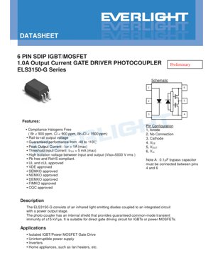
4.1 Pin Configuration and Function
The device uses a 6-pin SDIP package. The pinout is as follows:
- Pin 1: Anode of the input LED.
- Pin 2: No Connection (NC). Internally unconnected.
- Pin 3: Cathode of the input LED.
- Pin 4: VEE. The negative supply rail for the output stage. This can be ground (0V) or a negative voltage for IGBTs requiring negative turn-off bias.
- Pin 5: VOUT. The gate drive output pin. This connects directly to the gate of the IGBT or MOSFET, typically via a small gate resistor (Rg).
- Pin 6: VCC. The positive supply rail for the output stage.
4.2 Critical Application Note
A 0.1 μF bypass capacitor must be connected between pins 4 (VEE) and 6 (VCC), placed as close as physically possible to the photocoupler pins. This capacitor provides the high-frequency current required by the output stage during the fast switching transitions. Failure to include this capacitor or placing it too far away can lead to excessive ringing on the output, increased propagation delay, and potential malfunction due to supply bounce.
5. Soldering and Assembly Guidelines
The device has a maximum soldering temperature rating of 260°C for 10 seconds. This is compatible with standard lead-free (Pb-free) reflow soldering profiles. Standard ESD (Electrostatic Discharge) handling precautions must be observed, as the device contains sensitive semiconductor components. Recommended storage conditions are within the specified storage temperature range of -55°C to +125°C in a low-humidity, anti-static environment.
6. Application Design Considerations
6.1 Typical Application Circuit
A typical gate drive circuit involves an input current-limiting resistor (Rin) connected in series with the LED between a control signal (e.g., 3.3V or 5V from a microcontroller) and ground. The resistor value is calculated as Rin = (Vcontrol - VF) / IF. A value of 10-16 mA for IF is recommended. On the output side, the VCC and VEE supplies are derived from an isolated DC-DC converter. The output pin drives the gate through a small resistor (Rg, e.g., 2-10 Ω) which controls the switching speed and dampens ringing. An optional pull-down resistor (e.g., 10kΩ) from gate to source/emitter may be added for additional noise immunity when the driver is off.
6.2 Design Calculations and Trade-offs
- Gate Resistor Selection: A smaller Rg allows faster switching (lower switching losses) but increases peak current, EMI, and the risk of gate oscillation. The driver's 1A peak current capability sets a lower limit based on the supply voltage and gate threshold.
- Power Dissipation: The total power dissipation must be calculated and checked against the maximum rating of 300 mW. Dissipation comes from the input LED (IF*VF), the output IC quiescent current ((VCC-VEE)*ICC), and the switching losses in the output stage. At high switching frequencies (up to 50 kHz max), switching losses become significant.
- Layout Considerations: Minimize loop areas for high-current paths: 1) The path from the bypass capacitor (0.1μF) to VCC, VEE, and VOUT pins. 2) The gate drive loop from VOUT to the power device gate, through Rg, to the power device source/emitter, and back to VEE. Use short, wide traces or a ground plane.
7. Technical Comparison and Positioning
The ELS3150-G series is positioned as a robust, general-purpose gate driver photocoupler. Compared to basic optocouplers without a dedicated output stage, it offers significantly higher output current (1A vs. mA range), enabling direct drive of medium-power devices without an external buffer. Compared to some newer integrated driver ICs with higher levels of integration (e.g., desaturation detection, soft turn-off), it provides a fundamental, reliable isolation and driving function, often at a lower cost and with proven field reliability. Its key differentiators are the combination of 1A drive, high CMTI, wide temperature range, and compliance with major international safety standards.
8. Frequently Asked Questions (Based on Technical Parameters)
Q: Can I use a single +15V supply (VCC=15V, VEE=0V) to drive an IGBT?
A: Yes, this is a common configuration. The output will swing between nearly 0V and nearly 15V. Ensure the IGBT's gate-emitter voltage rating is not exceeded and that the 15V is sufficient to fully saturate the IGBT (check the IGBT's VGE specification).
Q: Why is my measured propagation delay longer than the typical 200 ns?
A: Propagation delay is tested with a specific load (Cg=10nF, Rg=10Ω). If your gate capacitance is larger or your gate resistor is larger, the delay will increase. Also, ensure the input current IF is at least 10 mA and the bypass capacitor is properly installed.
Q: The output voltage drop seems high when driving 1A. Is this normal?
A: Yes, refer to Figures 2 and 4. A voltage drop of 2-3V at 1A is typical, especially at temperature extremes. This reduces the effective gate drive voltage, which must be considered in the design. If a lower drop is critical, consider using a driver with a lower Rds(on) output stage or paralleling devices (with attention to skew).
9. Practical Application Example
Scenario: Driving a 600V/30A IGBT in a single-phase inverter leg for a motor drive.
The control signal from the DSP (3.3V) is connected to the photocoupler input via a 180Ω resistor (IF ≈ (3.3V-1.5V)/180Ω ≈ 10 mA). The output side uses an isolated flyback converter to generate +15V (VCC) and -5V (VEE) supplies, providing a 20V gate swing. A 0.1μF ceramic capacitor is placed directly across pins 4 and 6. The output (Pin 5) connects to the IGBT gate through a 4.7Ω gate resistor to control dV/dt and reduce EMI. The negative turn-off voltage helps prevent spurious turn-on due to Miller capacitance. The high CMTI rating ensures reliable operation despite the high dv/dt generated when the complementary IGBT in the leg switches.
10. Operating Principle
The device operates on the principle of optical isolation. An electrical input signal applied to the LED (Pins 1 & 3) causes it to emit infrared light. This light traverses an optically transparent isolation barrier (typically a molded plastic) and strikes a photodiode array integrated into the output-side IC. The photocurrent generated is processed by the IC's internal circuitry to control a totem-pole output stage consisting of a high-side and a low-side transistor. This output stage can source and sink current to rapidly charge and discharge the capacitive load presented by the power device's gate. The internal metallic shield between the LED and the detector IC capacitively decouples them, greatly enhancing immunity to fast common-mode voltage transients.
11. Industry Trends
The demand for gate driver photocouplers remains strong in industrial automation, renewable energy, and electric vehicle sectors, driven by the need for reliable high-voltage isolation. Key trends influencing this product category include: 1) Higher Integration: Incorporating advanced protection features like desaturation detection, active Miller clamp, and fault feedback channels into the isolated package. 2) Higher Speed and Lower Delay Skew: To support faster switching wide-bandgap semiconductors (SiC, GaN). 3) Enhanced Reliability Metrics: Longer operational lifetime predictions, higher maximum junction temperatures, and improved robustness against cosmic radiation for automotive and aerospace applications. 4) Package Miniaturization: Moving towards smaller surface-mount packages (like SO-8) with the same or better isolation ratings to save board space. The fundamental architecture of optical isolation, as exemplified by the ELS3150-G, continues to be a trusted and widely adopted solution due to its simplicity, noise immunity, and proven long-term reliability.
LED Specification Terminology
Complete explanation of LED technical terms
Photoelectric Performance
| Term | Unit/Representation | Simple Explanation | Why Important |
|---|---|---|---|
| Luminous Efficacy | lm/W (lumens per watt) | Light output per watt of electricity, higher means more energy efficient. | Directly determines energy efficiency grade and electricity cost. |
| Luminous Flux | lm (lumens) | Total light emitted by source, commonly called "brightness". | Determines if the light is bright enough. |
| Viewing Angle | ° (degrees), e.g., 120° | Angle where light intensity drops to half, determines beam width. | Affects illumination range and uniformity. |
| CCT (Color Temperature) | K (Kelvin), e.g., 2700K/6500K | Warmth/coolness of light, lower values yellowish/warm, higher whitish/cool. | Determines lighting atmosphere and suitable scenarios. |
| CRI / Ra | Unitless, 0–100 | Ability to render object colors accurately, Ra≥80 is good. | Affects color authenticity, used in high-demand places like malls, museums. |
| SDCM | MacAdam ellipse steps, e.g., "5-step" | Color consistency metric, smaller steps mean more consistent color. | Ensures uniform color across same batch of LEDs. |
| Dominant Wavelength | nm (nanometers), e.g., 620nm (red) | Wavelength corresponding to color of colored LEDs. | Determines hue of red, yellow, green monochrome LEDs. |
| Spectral Distribution | Wavelength vs intensity curve | Shows intensity distribution across wavelengths. | Affects color rendering and quality. |
Electrical Parameters
| Term | Symbol | Simple Explanation | Design Considerations |
|---|---|---|---|
| Forward Voltage | Vf | Minimum voltage to turn on LED, like "starting threshold". | Driver voltage must be ≥Vf, voltages add up for series LEDs. |
| Forward Current | If | Current value for normal LED operation. | Usually constant current drive, current determines brightness & lifespan. |
| Max Pulse Current | Ifp | Peak current tolerable for short periods, used for dimming or flashing. | Pulse width & duty cycle must be strictly controlled to avoid damage. |
| Reverse Voltage | Vr | Max reverse voltage LED can withstand, beyond may cause breakdown. | Circuit must prevent reverse connection or voltage spikes. |
| Thermal Resistance | Rth (°C/W) | Resistance to heat transfer from chip to solder, lower is better. | High thermal resistance requires stronger heat dissipation. |
| ESD Immunity | V (HBM), e.g., 1000V | Ability to withstand electrostatic discharge, higher means less vulnerable. | Anti-static measures needed in production, especially for sensitive LEDs. |
Thermal Management & Reliability
| Term | Key Metric | Simple Explanation | Impact |
|---|---|---|---|
| Junction Temperature | Tj (°C) | Actual operating temperature inside LED chip. | Every 10°C reduction may double lifespan; too high causes light decay, color shift. |
| Lumen Depreciation | L70 / L80 (hours) | Time for brightness to drop to 70% or 80% of initial. | Directly defines LED "service life". |
| Lumen Maintenance | % (e.g., 70%) | Percentage of brightness retained after time. | Indicates brightness retention over long-term use. |
| Color Shift | Δu′v′ or MacAdam ellipse | Degree of color change during use. | Affects color consistency in lighting scenes. |
| Thermal Aging | Material degradation | Deterioration due to long-term high temperature. | May cause brightness drop, color change, or open-circuit failure. |
Packaging & Materials
| Term | Common Types | Simple Explanation | Features & Applications |
|---|---|---|---|
| Package Type | EMC, PPA, Ceramic | Housing material protecting chip, providing optical/thermal interface. | EMC: good heat resistance, low cost; Ceramic: better heat dissipation, longer life. |
| Chip Structure | Front, Flip Chip | Chip electrode arrangement. | Flip chip: better heat dissipation, higher efficacy, for high-power. |
| Phosphor Coating | YAG, Silicate, Nitride | Covers blue chip, converts some to yellow/red, mixes to white. | Different phosphors affect efficacy, CCT, and CRI. |
| Lens/Optics | Flat, Microlens, TIR | Optical structure on surface controlling light distribution. | Determines viewing angle and light distribution curve. |
Quality Control & Binning
| Term | Binning Content | Simple Explanation | Purpose |
|---|---|---|---|
| Luminous Flux Bin | Code e.g., 2G, 2H | Grouped by brightness, each group has min/max lumen values. | Ensures uniform brightness in same batch. |
| Voltage Bin | Code e.g., 6W, 6X | Grouped by forward voltage range. | Facilitates driver matching, improves system efficiency. |
| Color Bin | 5-step MacAdam ellipse | Grouped by color coordinates, ensuring tight range. | Guarantees color consistency, avoids uneven color within fixture. |
| CCT Bin | 2700K, 3000K etc. | Grouped by CCT, each has corresponding coordinate range. | Meets different scene CCT requirements. |
Testing & Certification
| Term | Standard/Test | Simple Explanation | Significance |
|---|---|---|---|
| LM-80 | Lumen maintenance test | Long-term lighting at constant temperature, recording brightness decay. | Used to estimate LED life (with TM-21). |
| TM-21 | Life estimation standard | Estimates life under actual conditions based on LM-80 data. | Provides scientific life prediction. |
| IESNA | Illuminating Engineering Society | Covers optical, electrical, thermal test methods. | Industry-recognized test basis. |
| RoHS / REACH | Environmental certification | Ensures no harmful substances (lead, mercury). | Market access requirement internationally. |
| ENERGY STAR / DLC | Energy efficiency certification | Energy efficiency and performance certification for lighting. | Used in government procurement, subsidy programs, enhances competitiveness. |