Table of Contents
- 1. Product Overview
- 1.1 Core Advantages and Positioning
- 1.2 Target Applications
- 2. In-Depth Technical Parameter Analysis
- 2.1 Absolute Maximum Ratings
- 2.2 Electrical Characteristics (Input)
- 2.3 Electrical Characteristics (Output & Transfer)
- 2.4 Switching Characteristics
- 3. Mechanical and Package Information
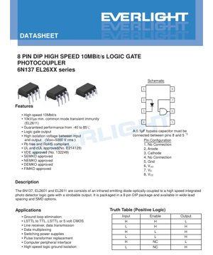
- 3.1 Pin Configuration (8-Pin DIP)
- 3.2 Package Options
- 4. Application Guidelines and Design Considerations
- 4.1 Critical Design Rules
- 4.2 Truth Table (Positive Logic)
- 4.3 Recommended Circuit for High CMTI (EL2611)
- 5. Performance Curves and Typical Characteristics
- 6. Soldering and Handling
- 7. Technical Comparison and Selection Guide
- 8. Principle of Operation
- 9. Frequently Asked Questions (FAQs)
- 10. Application Examples and Use Cases
- LED Specification Terminology
- Photoelectric Performance
- Electrical Parameters
- Thermal Management & Reliability
- Packaging & Materials
- Quality Control & Binning
- Testing & Certification
1. Product Overview
The 6N137, EL2601, and EL2611 are high-speed, logic gate output photocouplers (optoisolators). These devices consist of an infrared light-emitting diode (LED) optically coupled to a high-speed integrated photodetector with a strobable output. They are designed for applications requiring electrical isolation and high-speed digital signal transmission.
1.1 Core Advantages and Positioning
The primary advantage of this series is its combination of high-speed performance and robust isolation. With a data rate of up to 10 Mbit/s, it is suitable for modern digital communication interfaces. The devices offer a high common-mode transient immunity (CMTI), with the EL2611 variant rated for a minimum of 10 kV/μs, making them ideal for noisy industrial environments. The logic gate output simplifies interface with standard logic families like TTL and CMOS.
1.2 Target Applications
These photocouplers are targeted at applications requiring ground loop elimination, signal isolation in data transmission systems, and noise immunity in power electronics. Common use cases include:
- Isolation in switching power supplies and motor drives.
- Data line receivers and multiplexing systems.
- Replacement for pulse transformers in digital circuits.
- Computer peripheral interfaces and industrial control systems.
- General-purpose high-speed logic isolation.
2. In-Depth Technical Parameter Analysis
The following sections provide a detailed breakdown of the device's electrical and switching characteristics.
2.1 Absolute Maximum Ratings
These ratings define the stress limits beyond which permanent damage may occur. Key parameters include:
- Input Forward Current (IF): 50 mA maximum.
- Supply Voltage (VCC): 7.0 V maximum.
- Output Voltage (VO): 7.0 V maximum.
- Isolation Voltage (VISO): 5000 Vrms for 1 minute (test condition: pins 1-4 shorted together, pins 5-8 shorted together).
- Operating Temperature (TOPR): -40°C to +85°C.
- Storage Temperature (TSTG): -55°C to +125°C.
2.2 Electrical Characteristics (Input)
Parameters related to the input infrared LED:
- Forward Voltage (VF): Typically 1.4V, maximum 1.8V at IF = 10 mA.
- Reverse Voltage (VR): 5.0 V maximum.
- Temperature Coefficient of VF: Approximately -1.8 mV/°C.
- Input Capacitance (CIN): Typically 60 pF.
2.3 Electrical Characteristics (Output & Transfer)
Parameters related to the output detector and the overall signal transfer:
- Supply Current (High/Low): ICCH (output high) is typically 7 mA (max 10 mA). ICCL (output low) is typically 9 mA (max 13 mA).
- Enable Input Currents: IEH and IEL are typically below 1.6 mA.
- Low-Level Output Voltage (VOL): Typically 0.35V, maximum 0.6V under specified load conditions (ICL=13mA). This is a critical parameter for logic-level compatibility.
- Input Threshold Current (IFT): The LED current required to guarantee a logic-low output is typically 2.5 mA, maximum 5 mA.
2.4 Switching Characteristics
These parameters define the speed performance of the photocoupler, measured under standard conditions (VCC=5V, IF=7.5mA, CL=15pF, RL=350Ω).
- Propagation Delay (tPHL, tPLH): Typically 35-40 ns, with a maximum of 75 ns for both high-to-low and low-to-high transitions. This enables the 10 Mbit/s data rate.
- Pulse Width Distortion: |tPHL - tPLH| is typically 5 ns, maximum 35 ns. Lower distortion is better for preserving signal integrity.
- Rise/Fall Times (tr, tf): Output rise time is typically 40 ns, while fall time is typically a faster 10 ns.
- Enable Propagation Delay: The delay from the enable (VE) pin to the output is typically 15 ns.
- Common-Mode Transient Immunity (CMTI): This is a key differentiator. The 6N137 has no specified minimum. The EL2601 guarantees 5,000 V/μs. The EL2611 guarantees 10,000 V/μs under standard test and 20,000 V/μs with the recommended drive circuit (Fig. 15). High CMTI prevents noise from coupling across the isolation barrier.
3. Mechanical and Package Information
3.1 Pin Configuration (8-Pin DIP)
The device is offered in a standard 8-pin Dual In-line Package (DIP).
- No Connection (NC)
- Anode (A) of input LED
- Cathode (K) of input LED
- No Connection (NC)
- Ground (GND) for output side
- Output (VOUT)
- Enable Input (VE)
- Supply Voltage (VCC) for output side
3.2 Package Options
The datasheet mentions availability in wide-lead spacing and Surface-Mount Device (SMD) options, though specific package codes (e.g., SOIC-8) are not detailed in the provided excerpt.
4. Application Guidelines and Design Considerations
4.1 Critical Design Rules
- Bypass Capacitor: A 0.1 μF (or larger) capacitor with good high-frequency characteristics (ceramic or solid tantalum) must be connected between pins 8 (VCC) and 5 (GND), placed as close as possible to the device. This is essential for stable operation and minimizing noise.
- Enable Pin: The enable input (pin 7) has an internal pull-up resistor, so no external resistor is required. Driving it low (<0.8V) enables the output. Driving it high (>2.0V) forces the output high, regardless of the input LED state.
- Input Current: To ensure proper switching, the input LED current should be set according to the required speed and the IFT parameter. A typical operating current is 7.5-10 mA.
- Output Load: The standard test condition uses a 350Ω pull-up resistor to VCC. This value should be used as a reference for circuit design to meet the specified switching times.
4.2 Truth Table (Positive Logic)
The device functions as a non-inverting buffer when enabled. The truth table is as follows:
| Input (LED) | Enable (VE) | Output (VOUT) |
|---|---|---|
| H (ON) | H (High, >2.0V) | L (Low) |
| L (OFF) | H (High, >2.0V) | H (High) |
| H (ON) | L (Low, <0.8V) | H (High) |
| L (OFF) | L (Low, <0.8V) | H (High) |
| H (ON) | NC (Not Connected, internally pulled up) | L (Low) |
| L (OFF) | NC (Not Connected, internally pulled up) | H (High) |
4.3 Recommended Circuit for High CMTI (EL2611)
Figure 15 in the datasheet shows a specific drive circuit recommended for the EL2611 family to achieve its highest specified CMTI of 20,000 V/μs. This circuit typically involves careful management of the input LED drive path to minimize parasitic coupling.
5. Performance Curves and Typical Characteristics
The datasheet includes a section for \"Typical Electro-Optical Characteristics Curves.\" While the specific graphs are not provided in the text excerpt, such curves typically illustrate relationships critical for design:
- Current Transfer Ratio (CTR) vs. Forward Current: Shows the efficiency of the optical coupling.
- Propagation Delay vs. Forward Current: Demonstrates how speed varies with LED drive current.
- Output Voltage vs. Temperature: Indicates thermal stability of the output logic levels.
- Common-Mode Transient Immunity vs. Frequency: Shows the CMTI performance across different noise frequencies.
Designers should consult these graphs to optimize performance for their specific operating conditions (temperature, required speed).
6. Soldering and Handling
The Absolute Maximum Ratings specify a soldering temperature (TSOL) of 260°C for 10 seconds. This aligns with typical lead-free reflow soldering profiles. Standard ESD (Electrostatic Discharge) precautions should be observed when handling these semiconductor devices.
7. Technical Comparison and Selection Guide
The 6N137, EL2601, and EL2611 share a common pinout and core functionality but differ in a key specification:
- 6N137: Base high-speed model. CMTI is not guaranteed to a specific minimum level.
- EL2601: Enhanced model with a guaranteed minimum CMTI of 5,000 V/μs.
- EL2611: Premium model with a guaranteed minimum CMTI of 10,000 V/μs (20,000 V/μs with recommended circuit).
Selection Advice: For general-purpose digital isolation in benign environments, the 6N137 may be sufficient. For industrial motor drives, power inverters, or any environment with high-voltage switching noise (dV/dt), the EL2601 or EL2611 should be selected based on the noise immunity required. The EL2611 with its specialized drive circuit offers the highest robustness.
8. Principle of Operation
A photocoupler provides galvanic isolation by using light as the signal transmission medium. An electrical signal drives the input Infrared LED, causing it to emit light. This light crosses an isolation gap (often a transparent dielectric) and strikes a photodetector integrated with a logic gate circuit on the output side. The detector converts the light back into an electrical signal, which is then conditioned by the logic gate (with enable/disable functionality) to produce a clean digital output. The physical separation between the LED and the detector provides the high isolation voltage rating.
9. Frequently Asked Questions (FAQs)
Q: What is the purpose of the enable (VE) pin?
A: The enable pin allows the output to be forced into a high state, effectively muting the signal from the input. This can be useful for bus sharing, fault conditions, or power-saving modes.
Q: Can I drive the input LED directly from a microcontroller pin?
A: Possibly, but it depends on the microcontroller's output current capability and voltage. The typical VF is 1.4V at 10 mA. A series current-limiting resistor is always required. Ensure the MCU pin can source/sink the required IF (e.g., 7.5-10 mA for full speed).
Q: Why is the bypass capacitor so critical?
A> The high-speed switching of the internal detector circuit can cause sudden current spikes on the VCC line. The local bypass capacitor supplies this transient current, preventing voltage droops that could cause output glitches or false triggering, and also helps shunt high-frequency noise.
Q: How do I choose between the 6N137, EL2601, and EL2611?
A: The primary differentiator is Common-Mode Transient Immunity (CMTI). If your application involves significant voltage swings across the isolation barrier (e.g., in a motor drive), choose the EL2601 or EL2611. For simple digital isolation in low-noise settings, the 6N137 may be adequate. Always refer to the specific CMTI requirements of your system.
10. Application Examples and Use Cases
Case 1: Isolated RS-485/422 Interface: The photocoupler can be used to isolate the data lines (TxD, RxD) and/or the direction control line of a UART-to-RS485 transceiver. This breaks ground loops and protects the sensitive logic side from faults on the long bus lines. The high speed ensures no bottleneck in data throughput.
Case 2: Gate Drive Isolation in a Switch-Mode Power Supply (SMPS): In a half-bridge or full-bridge topology, the high-side MOSFET/IGBT gate driver needs a signal referenced to a floating switch node. A photocoupler like the EL2611 can transmit the PWM control signal from the low-side controller to the high-side driver, providing both level shifting and isolation. Its high CMTI is crucial to ignore the large dV/dt noise from the switching node.
Case 3: Digital Input Module for PLC: Industrial Programmable Logic Controllers (PLCs) read signals from sensors and switches in harsh environments. Photocouplers are used on every digital input channel to isolate the field wiring (24V sensors) from the internal PLC logic (3.3V/5V). They provide protection against overvoltage, noise, and wiring errors.
LED Specification Terminology
Complete explanation of LED technical terms
Photoelectric Performance
| Term | Unit/Representation | Simple Explanation | Why Important |
|---|---|---|---|
| Luminous Efficacy | lm/W (lumens per watt) | Light output per watt of electricity, higher means more energy efficient. | Directly determines energy efficiency grade and electricity cost. |
| Luminous Flux | lm (lumens) | Total light emitted by source, commonly called "brightness". | Determines if the light is bright enough. |
| Viewing Angle | ° (degrees), e.g., 120° | Angle where light intensity drops to half, determines beam width. | Affects illumination range and uniformity. |
| CCT (Color Temperature) | K (Kelvin), e.g., 2700K/6500K | Warmth/coolness of light, lower values yellowish/warm, higher whitish/cool. | Determines lighting atmosphere and suitable scenarios. |
| CRI / Ra | Unitless, 0–100 | Ability to render object colors accurately, Ra≥80 is good. | Affects color authenticity, used in high-demand places like malls, museums. |
| SDCM | MacAdam ellipse steps, e.g., "5-step" | Color consistency metric, smaller steps mean more consistent color. | Ensures uniform color across same batch of LEDs. |
| Dominant Wavelength | nm (nanometers), e.g., 620nm (red) | Wavelength corresponding to color of colored LEDs. | Determines hue of red, yellow, green monochrome LEDs. |
| Spectral Distribution | Wavelength vs intensity curve | Shows intensity distribution across wavelengths. | Affects color rendering and quality. |
Electrical Parameters
| Term | Symbol | Simple Explanation | Design Considerations |
|---|---|---|---|
| Forward Voltage | Vf | Minimum voltage to turn on LED, like "starting threshold". | Driver voltage must be ≥Vf, voltages add up for series LEDs. |
| Forward Current | If | Current value for normal LED operation. | Usually constant current drive, current determines brightness & lifespan. |
| Max Pulse Current | Ifp | Peak current tolerable for short periods, used for dimming or flashing. | Pulse width & duty cycle must be strictly controlled to avoid damage. |
| Reverse Voltage | Vr | Max reverse voltage LED can withstand, beyond may cause breakdown. | Circuit must prevent reverse connection or voltage spikes. |
| Thermal Resistance | Rth (°C/W) | Resistance to heat transfer from chip to solder, lower is better. | High thermal resistance requires stronger heat dissipation. |
| ESD Immunity | V (HBM), e.g., 1000V | Ability to withstand electrostatic discharge, higher means less vulnerable. | Anti-static measures needed in production, especially for sensitive LEDs. |
Thermal Management & Reliability
| Term | Key Metric | Simple Explanation | Impact |
|---|---|---|---|
| Junction Temperature | Tj (°C) | Actual operating temperature inside LED chip. | Every 10°C reduction may double lifespan; too high causes light decay, color shift. |
| Lumen Depreciation | L70 / L80 (hours) | Time for brightness to drop to 70% or 80% of initial. | Directly defines LED "service life". |
| Lumen Maintenance | % (e.g., 70%) | Percentage of brightness retained after time. | Indicates brightness retention over long-term use. |
| Color Shift | Δu′v′ or MacAdam ellipse | Degree of color change during use. | Affects color consistency in lighting scenes. |
| Thermal Aging | Material degradation | Deterioration due to long-term high temperature. | May cause brightness drop, color change, or open-circuit failure. |
Packaging & Materials
| Term | Common Types | Simple Explanation | Features & Applications |
|---|---|---|---|
| Package Type | EMC, PPA, Ceramic | Housing material protecting chip, providing optical/thermal interface. | EMC: good heat resistance, low cost; Ceramic: better heat dissipation, longer life. |
| Chip Structure | Front, Flip Chip | Chip electrode arrangement. | Flip chip: better heat dissipation, higher efficacy, for high-power. |
| Phosphor Coating | YAG, Silicate, Nitride | Covers blue chip, converts some to yellow/red, mixes to white. | Different phosphors affect efficacy, CCT, and CRI. |
| Lens/Optics | Flat, Microlens, TIR | Optical structure on surface controlling light distribution. | Determines viewing angle and light distribution curve. |
Quality Control & Binning
| Term | Binning Content | Simple Explanation | Purpose |
|---|---|---|---|
| Luminous Flux Bin | Code e.g., 2G, 2H | Grouped by brightness, each group has min/max lumen values. | Ensures uniform brightness in same batch. |
| Voltage Bin | Code e.g., 6W, 6X | Grouped by forward voltage range. | Facilitates driver matching, improves system efficiency. |
| Color Bin | 5-step MacAdam ellipse | Grouped by color coordinates, ensuring tight range. | Guarantees color consistency, avoids uneven color within fixture. |
| CCT Bin | 2700K, 3000K etc. | Grouped by CCT, each has corresponding coordinate range. | Meets different scene CCT requirements. |
Testing & Certification
| Term | Standard/Test | Simple Explanation | Significance |
|---|---|---|---|
| LM-80 | Lumen maintenance test | Long-term lighting at constant temperature, recording brightness decay. | Used to estimate LED life (with TM-21). |
| TM-21 | Life estimation standard | Estimates life under actual conditions based on LM-80 data. | Provides scientific life prediction. |
| IESNA | Illuminating Engineering Society | Covers optical, electrical, thermal test methods. | Industry-recognized test basis. |
| RoHS / REACH | Environmental certification | Ensures no harmful substances (lead, mercury). | Market access requirement internationally. |
| ENERGY STAR / DLC | Energy efficiency certification | Energy efficiency and performance certification for lighting. | Used in government procurement, subsidy programs, enhances competitiveness. |