Table of Contents
- 1. Product Overview
- 2. Technical Specifications Deep Dive
- 2.1 Absolute Maximum Ratings
- 2.2 Electro-Optical Characteristics
- 3. Performance Curve Analysis
- 3.1 Forward Current vs. Ambient Temperature
- 3.2 Spectral Distribution
- 3.3 Radiant Intensity vs. Forward Current
- 3.4 Forward Current vs. Forward Voltage (I-V Curve)
- 3.5 Relative Radiant Intensity vs. Angular Displacement
- 4. Mechanical and Package Information
- 5. Soldering and Assembly Guidelines
- 5.1 Reflow Soldering
- 5.2 Hand Soldering
- 5.3 Storage and Moisture Sensitivity
- 6. Packaging and Ordering Information
- 7. Application Suggestions
- 7.1 Typical Application Scenarios
- 7.2 Design Considerations
- 8. Technical Comparison and Differentiation
- 9. Frequently Asked Questions (Based on Technical Parameters)
- 10. Design and Usage Case Study
- 11. Operational Principle
- 12. Technology Trends
- LED Specification Terminology
- Photoelectric Performance
- Electrical Parameters
- Thermal Management & Reliability
- Packaging & Materials
- Quality Control & Binning
- Testing & Certification
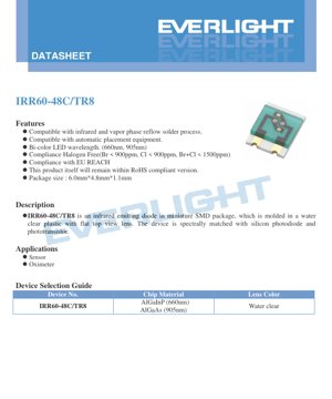
1. Product Overview
The IRR60-48C/TR8 is a miniature surface-mount device (SMD) infrared emitting diode. It is a bi-color component featuring two distinct semiconductor chips within a single package: one emitting at 660nm (red, AlGaInP material) and another emitting at 905nm (infrared, AlGaAs material). The device is encapsulated in a water-clear plastic package with a flat-top lens, designed for compatibility with automated pick-and-place assembly systems and standard infrared or vapor phase reflow soldering processes.
The primary design objective of this component is spectral matching with silicon-based photodetectors such as photodiodes and phototransistors. This characteristic makes it particularly suitable for sensing applications where precise optical coupling is required. The device adheres to modern environmental standards, being halogen-free and compliant with RoHS and EU REACH regulations.
2. Technical Specifications Deep Dive
2.1 Absolute Maximum Ratings
These ratings define the limits beyond which permanent damage to the device may occur. Operation under these conditions is not guaranteed.
- Continuous Forward Current (IF): 30 mA for both wavelengths. This is the maximum DC current that can be applied continuously.
- Peak Forward Current (IFP): 150 mA. This rating applies only under pulsed conditions with a pulse width ≤10μs and a duty cycle ≤1%.
- Reverse Voltage (VR): 5 V. Exceeding this voltage in reverse bias can cause junction breakdown.
- Power Dissipation (Pd): 70 mW for the 660nm chip and 50 mW for the 905nm chip, measured at or below 25°C ambient temperature. This difference reflects the typical efficiency and thermal characteristics of the different semiconductor materials.
- Thermal Resistance, Junction-to-Ambient (Rθj-a): 550 K/W. This parameter indicates how effectively heat is transferred from the semiconductor junction to the surrounding environment. A lower value signifies better heat dissipation.
- Operating & Storage Temperature Range: -25°C to +85°C.
- Soldering Temperature (Tsol): 260°C maximum for a duration not exceeding 5 seconds, typical for lead-free reflow processes.
2.2 Electro-Optical Characteristics
These are the typical performance parameters measured at 25°C with a forward current of 20mA, unless otherwise specified.
- Radiant Intensity (IE): This is the optical power emitted per unit solid angle (steradian). For the 660nm (Red) chip, the typical value is 2.3 mW/sr (min 1.0). For the 905nm (IR) chip, the typical value is 1.0 mW/sr (min 0.5).
- Total Radiated Power (Po): The total optical power emitted in all directions. Typical values are 7.0 mW for Red and 3.0 mW for IR.
- Peak Wavelength (λp): The wavelength at which the emitted radiation is strongest. The Red chip is centered at 660nm (range 657-663nm). The IR chip is centered at 905nm (range 895-915nm).
- Spectral Bandwidth (Δλ): The width of the emission spectrum at half its maximum intensity (Full Width at Half Maximum - FWHM). Typical values are 20nm for Red and 60nm for IR. The broader bandwidth of the IR chip is characteristic of AlGaAs materials.
- Forward Voltage (VF): The voltage drop across the diode when conducting. The Red chip typically requires 2.10V (range 1.80-2.50V). The IR chip typically requires 1.40V (range 1.10-1.60V). This difference is crucial for circuit design, especially when driving both chips from a common source.
- Viewing Angle (2θ1/2): The angular spread where the radiant intensity is at least half of its peak value. The Red chip has a typical viewing angle of 140°, while the IR chip has 130°. The flat-top lens contributes to this wide viewing angle.
3. Performance Curve Analysis
3.1 Forward Current vs. Ambient Temperature
The derating curves show the maximum allowable continuous forward current decreasing as ambient temperature increases. This is a critical design consideration to prevent thermal runaway. The curves for both the Red and IR chips follow a similar negative slope, emphasizing the need for adequate thermal management in high-temperature environments or high-current applications.
3.2 Spectral Distribution
The spectral graphs illustrate the relative radiant intensity across wavelengths. The 660nm Red emission shows a sharp, narrow peak characteristic of AlGaInP materials. The 905nm IR emission shows a broader, Gaussian-like distribution typical for AlGaAs. This spectral purity (for Red) and bandwidth (for IR) are key for sensor system design, affecting filter selection and signal-to-noise ratio.
3.3 Radiant Intensity vs. Forward Current
These plots demonstrate a near-linear relationship between drive current and optical output for both chips within the standard operating range. This linearity simplifies optical output control in analog modulation applications. The slope of the line (efficiency) differs between the two wavelengths.
3.4 Forward Current vs. Forward Voltage (I-V Curve)
The I-V curves show the exponential relationship typical of diodes. The turn-on voltage is clearly visible and differs between the two chips (higher for Red). The curves are measured under pulsed conditions (100μs pulse, 1/100 duty cycle) to minimize self-heating effects, providing the most accurate representation of the junction characteristics.
3.5 Relative Radiant Intensity vs. Angular Displacement
These polar plots visually represent the viewing angle. The intensity distribution is roughly Lambertian (cosine-like) for both chips, with the Red being slightly wider. This information is vital for designing optical systems to ensure proper illumination coverage or alignment with a detector.
4. Mechanical and Package Information
The device is housed in a compact SMD package measuring 6.0mm in length, 4.8mm in width, and 1.1mm in height. The package outline drawing provides critical dimensions for PCB footprint design, including pad size, placement, and keep-out areas. The component features a water-clear molded plastic body with a flat top, which acts as a lens. The polarity is indicated by the package marking and must be observed during placement to ensure correct electrical operation.
5. Soldering and Assembly Guidelines
5.1 Reflow Soldering
The component is compatible with lead-free (Pb-free) reflow soldering profiles with a peak temperature of 260°C. It is critical to adhere to the recommended temperature-time profile to avoid thermal shock or damage to the plastic package. Reflow soldering should not be performed more than two times on the same device. Stress on the LED body during heating and warping of the circuit board after soldering must be avoided.
5.2 Hand Soldering
If hand soldering is necessary for repair, extreme caution is required. The soldering iron tip temperature should be below 350°C, and contact time per terminal should not exceed 3 seconds. A low-power iron (≤25W) is recommended. A minimum interval of 2 seconds should be left between soldering each terminal. The use of a double-head soldering iron for removal is suggested to minimize thermal stress, but its effect on device characteristics should be verified beforehand.
5.3 Storage and Moisture Sensitivity
The device is moisture-sensitive. Precautions include:
- Do not open the moisture-proof bag until ready for use.
- Store unopened bags at ≤30°C and ≤90% RH. Use within one year.
- After opening, store at ≤30°C and ≤60% RH. Use within 24 hours.
- If the storage time is exceeded or the desiccant indicates moisture ingress, a baking treatment at 60±5°C for at least 24 hours is required before reflow.
6. Packaging and Ordering Information
The device is supplied on embossed carrier tape for automated handling. The standard reel contains 1000 pieces. The carrier tape dimensions are specified to ensure compatibility with standard feeder systems. The moisture-resistant packaging consists of an aluminum laminate bag containing desiccant and a humidity indicator card. The bag label includes fields for Customer Part Number (CPN), Production Number (P/N), quantity, rank codes (CAT, HUE), reference, lot number, and country of origin.
7. Application Suggestions
7.1 Typical Application Scenarios
- Optical Sensors: The dual wavelengths enable use in reflective or transmissive sensors for object detection, counting, or position sensing. The 905nm wavelength is often used where visible light is undesirable, while the 660nm red can serve as a visible indicator or for specific photometric sensing.
- Medical Pulse Oximetry: The 660nm and 905nm (or 940nm) wavelengths are standard in pulse oximeters for measuring blood oxygen saturation (SpO2). The device's spectral matching to silicon detectors is essential for this application.
- Industrial Automation: Used in optical encoders, edge detection systems, and safety curtains.
7.2 Design Considerations
- Current Limiting: An external series resistor is mandatory for operation from a voltage source. The I-V curve's steep slope means a small voltage change causes a large current change, which can instantly destroy the LED.
- Thermal Management:** The specified thermal resistance (550 K/W) is relatively high. For continuous operation at high currents or in warm environments, PCB layout with adequate copper area for heat sinking is recommended to maintain junction temperature within limits.
- Optical Design: The wide viewing angle may require secondary optics (lenses, apertures) to collimate or focus the light for specific sensing tasks. The water-clear lens is suitable for applications where the exact emission pattern is not critical or where external optics are used.
- Drive Circuitry: The different forward voltages of the two chips must be considered if they are to be driven independently or multiplexed. Constant current drivers are preferred over constant voltage for stable optical output.
8. Technical Comparison and Differentiation
The IRR60-48C/TR8's primary differentiation lies in its dual-wavelength, single-package design. Compared to using two separate SMD LEDs, this offers significant advantages:
- Space Savings: Reduces PCB footprint by 50%.
- Simplified Assembly: Only one component to place, improving manufacturing throughput and reducing placement cost.
- Improved Alignment: The two emission points are co-located within the same package, ensuring perfect spatial alignment for applications requiring both wavelengths to illuminate the same spot. This is critical in devices like pulse oximeters.
- Material Compatibility: The use of AlGaInP for red offers higher efficiency and better spectral purity compared to older technologies like GaAsP, while the AlGaAs IR chip provides strong output in the near-infrared region.
9. Frequently Asked Questions (Based on Technical Parameters)
Q: Can I drive both LED chips simultaneously at their maximum continuous current of 30mA each?
A: No. The total power dissipation must be considered. Simultaneous operation at 30mA would likely exceed the package's thermal dissipation capability, leading to overheating. Derating based on ambient temperature and application-specific duty cycles is necessary.
Q: Why is the radiant intensity for the IR chip lower than the Red chip at the same current?
A> This is primarily due to the difference in eye sensitivity (photopic vs. radiometric measurement) and the inherent conversion efficiency of the different semiconductor materials (AlGaAs vs. AlGaInP) at their respective wavelengths. The Total Radiated Power metric provides a better comparison of total optical output.
Q: The datasheet shows a soldering temperature of 260°C, but my reflow profile peaks at 245°C. Is this acceptable?
A: Yes, a peak temperature of 245°C is acceptable and may be preferable as it subjects the component to less thermal stress, provided the time above liquidus (TAL) is sufficient for proper solder joint formation.
Q: How critical is the 24-hour use-after-opening window?
A: It is critical for reliable reflow soldering. Moisture absorbed into the plastic package can vaporize during reflow, causing internal delamination, cracking ("popcorning"), or bond wire damage. Adhering to this guideline is essential for high yield in manufacturing.
10. Design and Usage Case Study
Scenario: Designing a Reflective Object Sensor
In a typical application detecting a white object on a black conveyor belt, the IRR60-48C/TR8 would be paired with a silicon phototransistor. The 905nm IR chip would be used for primary sensing to avoid interference from ambient visible light. A constant current source set to 20mA would drive the LED. The light reflects off the object and is detected by the phototransistor, whose output signal is conditioned by an amplifier/comparator circuit. The wide 130° viewing angle of the IR chip ensures a generous detection field, reducing alignment precision requirements. The designer must include a current-limiting resistor if using a voltage source, ensure the PCB layout provides some thermal relief, and follow the strict moisture handling procedures before the board goes through reflow soldering.
11. Operational Principle
Light emission in the IRR60-48C/TR8 is based on electroluminescence in semiconductor materials. When a forward bias voltage exceeding the chip's bandgap energy is applied, electrons and holes are injected into the active region of the semiconductor where they recombine. This recombination releases energy in the form of photons (light). The wavelength (color) of the emitted light is determined by the bandgap energy of the semiconductor material: AlGaInP for 660nm (red) and AlGaAs for 905nm (infrared). The water-clear epoxy package encapsulates the chip, provides mechanical protection, and its shaped top surface acts as a primary lens to control the emission pattern.
12. Technology Trends
The development of SMD LEDs like the IRR60-48C/TR8 follows several industry trends:
- Miniaturization: Continued reduction in package size (e.g., from 0603 to 0402) to enable denser electronic assemblies.
- Multi-Chip Integration: Combining multiple wavelengths or even different device types (LEDs and photodiodes) into single packages for smarter, more compact sensor modules.
- Increased Efficiency: Ongoing improvements in internal quantum efficiency and light extraction from the semiconductor material and package, leading to higher optical output for the same electrical input.
- Enhanced Reliability: Advancements in packaging materials and processes to withstand higher reflow temperatures, harsher environmental conditions, and provide longer operational lifetimes.
- Standardization: Wider adoption of standardized footprints and optical characteristics to improve interchangeability and simplify design for engineers.
LED Specification Terminology
Complete explanation of LED technical terms
Photoelectric Performance
| Term | Unit/Representation | Simple Explanation | Why Important |
|---|---|---|---|
| Luminous Efficacy | lm/W (lumens per watt) | Light output per watt of electricity, higher means more energy efficient. | Directly determines energy efficiency grade and electricity cost. |
| Luminous Flux | lm (lumens) | Total light emitted by source, commonly called "brightness". | Determines if the light is bright enough. |
| Viewing Angle | ° (degrees), e.g., 120° | Angle where light intensity drops to half, determines beam width. | Affects illumination range and uniformity. |
| CCT (Color Temperature) | K (Kelvin), e.g., 2700K/6500K | Warmth/coolness of light, lower values yellowish/warm, higher whitish/cool. | Determines lighting atmosphere and suitable scenarios. |
| CRI / Ra | Unitless, 0–100 | Ability to render object colors accurately, Ra≥80 is good. | Affects color authenticity, used in high-demand places like malls, museums. |
| SDCM | MacAdam ellipse steps, e.g., "5-step" | Color consistency metric, smaller steps mean more consistent color. | Ensures uniform color across same batch of LEDs. |
| Dominant Wavelength | nm (nanometers), e.g., 620nm (red) | Wavelength corresponding to color of colored LEDs. | Determines hue of red, yellow, green monochrome LEDs. |
| Spectral Distribution | Wavelength vs intensity curve | Shows intensity distribution across wavelengths. | Affects color rendering and quality. |
Electrical Parameters
| Term | Symbol | Simple Explanation | Design Considerations |
|---|---|---|---|
| Forward Voltage | Vf | Minimum voltage to turn on LED, like "starting threshold". | Driver voltage must be ≥Vf, voltages add up for series LEDs. |
| Forward Current | If | Current value for normal LED operation. | Usually constant current drive, current determines brightness & lifespan. |
| Max Pulse Current | Ifp | Peak current tolerable for short periods, used for dimming or flashing. | Pulse width & duty cycle must be strictly controlled to avoid damage. |
| Reverse Voltage | Vr | Max reverse voltage LED can withstand, beyond may cause breakdown. | Circuit must prevent reverse connection or voltage spikes. |
| Thermal Resistance | Rth (°C/W) | Resistance to heat transfer from chip to solder, lower is better. | High thermal resistance requires stronger heat dissipation. |
| ESD Immunity | V (HBM), e.g., 1000V | Ability to withstand electrostatic discharge, higher means less vulnerable. | Anti-static measures needed in production, especially for sensitive LEDs. |
Thermal Management & Reliability
| Term | Key Metric | Simple Explanation | Impact |
|---|---|---|---|
| Junction Temperature | Tj (°C) | Actual operating temperature inside LED chip. | Every 10°C reduction may double lifespan; too high causes light decay, color shift. |
| Lumen Depreciation | L70 / L80 (hours) | Time for brightness to drop to 70% or 80% of initial. | Directly defines LED "service life". |
| Lumen Maintenance | % (e.g., 70%) | Percentage of brightness retained after time. | Indicates brightness retention over long-term use. |
| Color Shift | Δu′v′ or MacAdam ellipse | Degree of color change during use. | Affects color consistency in lighting scenes. |
| Thermal Aging | Material degradation | Deterioration due to long-term high temperature. | May cause brightness drop, color change, or open-circuit failure. |
Packaging & Materials
| Term | Common Types | Simple Explanation | Features & Applications |
|---|---|---|---|
| Package Type | EMC, PPA, Ceramic | Housing material protecting chip, providing optical/thermal interface. | EMC: good heat resistance, low cost; Ceramic: better heat dissipation, longer life. |
| Chip Structure | Front, Flip Chip | Chip electrode arrangement. | Flip chip: better heat dissipation, higher efficacy, for high-power. |
| Phosphor Coating | YAG, Silicate, Nitride | Covers blue chip, converts some to yellow/red, mixes to white. | Different phosphors affect efficacy, CCT, and CRI. |
| Lens/Optics | Flat, Microlens, TIR | Optical structure on surface controlling light distribution. | Determines viewing angle and light distribution curve. |
Quality Control & Binning
| Term | Binning Content | Simple Explanation | Purpose |
|---|---|---|---|
| Luminous Flux Bin | Code e.g., 2G, 2H | Grouped by brightness, each group has min/max lumen values. | Ensures uniform brightness in same batch. |
| Voltage Bin | Code e.g., 6W, 6X | Grouped by forward voltage range. | Facilitates driver matching, improves system efficiency. |
| Color Bin | 5-step MacAdam ellipse | Grouped by color coordinates, ensuring tight range. | Guarantees color consistency, avoids uneven color within fixture. |
| CCT Bin | 2700K, 3000K etc. | Grouped by CCT, each has corresponding coordinate range. | Meets different scene CCT requirements. |
Testing & Certification
| Term | Standard/Test | Simple Explanation | Significance |
|---|---|---|---|
| LM-80 | Lumen maintenance test | Long-term lighting at constant temperature, recording brightness decay. | Used to estimate LED life (with TM-21). |
| TM-21 | Life estimation standard | Estimates life under actual conditions based on LM-80 data. | Provides scientific life prediction. |
| IESNA | Illuminating Engineering Society | Covers optical, electrical, thermal test methods. | Industry-recognized test basis. |
| RoHS / REACH | Environmental certification | Ensures no harmful substances (lead, mercury). | Market access requirement internationally. |
| ENERGY STAR / DLC | Energy efficiency certification | Energy efficiency and performance certification for lighting. | Used in government procurement, subsidy programs, enhances competitiveness. |