1. Product Overview
The ELS680-G series represents a family of high-performance, intelligent power and gate drive interface photocouplers. These devices are engineered to provide robust electrical isolation and reliable signal transmission between low-voltage control circuits and high-voltage power stages, such as those found in motor drives and industrial inverters. The core function is to translate a logic-level input signal into a corresponding, isolated output signal capable of directly driving the gate of an IGBT or MOSFET, or interfacing with an Intelligent Power Module (IPM).
The primary application is to replace discrete optocoupler and driver circuits, simplifying design, improving reliability, and enhancing noise immunity in high-power switching environments. The integrated totem-pole output stage is a key feature, eliminating the need for an external pull-up resistor and providing sufficient current sourcing and sinking capability for direct gate drive.
1.1 Core Advantages and Target Market
The ELS680-G series offers several distinct advantages for power electronics design. First is the high isolation voltage of 5000 Vrms, which provides a critical safety margin and meets stringent requirements for industrial equipment. Second, the device is compliant with halogen-free standards (Br < 900 ppm, Cl < 900 ppm, Br+Cl < 1500 ppm), making it suitable for environmentally conscious applications. It is also Pb-free and RoHS compliant.
The target markets for this component are primarily industrial automation and power conversion. Specific applications include AC and Brushless DC motor drives, industrial inverters, uninterruptible power supplies (UPS), and solar inverters. Any system requiring reliable, isolated control signals for high-voltage power switches is a potential application area.
2. Technical Parameter Deep-Dive and Objective Interpretation
This section provides a detailed analysis of the electrical and performance characteristics specified in the datasheet. Understanding these parameters is crucial for reliable circuit design.
2.1 Absolute Maximum Ratings
The Absolute Maximum Ratings define the stress limits beyond which permanent damage to the device may occur. Operating continuously at or near these limits is not recommended. Key ratings include: Input Forward Current (IF) of 25 mA, Output Average Current (IO(AVG)) of 60 mA, and Supply Voltage (VCC) of 30 V. The total device power dissipation (PTOT) is limited to 350 mW. The isolation voltage (VISO) is rated at 5000 Vrms for one minute, tested under specific pin-shorting conditions. The operating temperature range is from -40°C to +100°C.
2.2 Electrical Characteristics
These parameters define the device's performance under normal operating conditions across the specified temperature range.
2.2.1 Input Characteristics
The input is an infrared Light Emitting Diode (LED). The typical Forward Voltage (VF) is 1.5V at a forward current (IF) of 10 mA, with a maximum of 1.8V. The Input Threshold Current (IFT) is a critical parameter, specifying the minimum LED current required to guarantee a valid logic-low output. The datasheet specifies a maximum IFT of 5 mA (typical 2.5 mA) at VCC=4.5V. Designers must ensure the driving circuit can provide at least this current for reliable operation.
2.2.2 Output and Transfer Characteristics
The output is a high-speed integrated photo-detector with a totem-pole configuration. Key parameters include: High-Level Output Voltage (VOH), which is typically very close to VCC (VCC - 0.5V min), and Low-Level Output Voltage (VOL), which is typically very close to VEE (VEE + 0.5V max). The supply currents (ICCH, ICCL) are both specified with a maximum of 3.2 mA. The Short Circuit Output Currents (IOSL, IOSH) indicate the output stage's current limiting capability, rated at ±60 mA minimum/maximum.
2.3 Switching Characteristics
These parameters define the timing performance of the photocoupler, critical for high-frequency switching applications.
- Propagation Delay (tPHL, tPLH): The time from the input LED current transition to the corresponding output transition. Typical values are 130 ns (tPHL) and 140 ns (tPLH), with maximums of 350 ns.
- Pulse Width Distortion (PWD): The absolute difference between tPHL and tPLH. A low PWD (max 250 ns) is important for maintaining signal integrity in precision timing applications.
- Rise/Fall Time (tr, tf): The output signal edge speeds, typically 9 ns and 6 ns respectively.
- Common Mode Transient Immunity (CMH, CML): This is a vital parameter for noise immunity. It specifies the minimum dV/dt (10 kV/µs typical) of a common-mode voltage spike that the device can withstand without causing an output glitch. High CMTI is essential in noisy motor drive environments.
3. Performance Curve Analysis and Design Considerations
While explicit performance curves are not provided in the extracted text, the datasheet implies several key relationships that designers must consider.
3.1 Temperature Dependence
Most electrical and switching characteristics are specified over the full -40°C to +100°C temperature range. Designers should note that parameters like forward voltage (VF), threshold current (IFT), and propagation delays will vary with temperature. For robust design, calculations should be based on the minimum and maximum limits, not just typical values.
3.2 Power Supply and Bypassing
The datasheet explicitly mandates the use of a 0.1 µF (or larger) bypass capacitor between the VCC (pin 6) and VEE (pin 4) pins. This capacitor must have good high-frequency characteristics (e.g., ceramic) and be placed as close as possible to the device pins. This is non-negotiable for achieving the specified switching performance and common-mode transient immunity. The capacitor provides a local charge reservoir for the output stage's transient current demands and helps shunt high-frequency noise.
4. Mechanical and Package Information
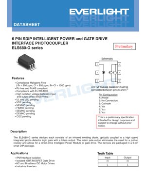
4.1 Pin Configuration and Function
The device is housed in a 6-pin Small Dual In-line Package (SDIP). The pinout is as follows: Pin 1: Anode of input LED; Pin 2: No Connection; Pin 3: Cathode of input LED; Pin 4: VEE (Output ground/reference); Pin 5: Vout (Output signal); Pin 6: VCC (Output supply voltage).
4.2 Package Dimensions and PCB Layout
The datasheet includes detailed mechanical drawings for the \"P Type\" surface mount lead form. Critical dimensions include body size, lead spacing, and standoff height. A recommended pad layout for surface mounting is also provided. Following this land pattern is essential for reliable soldering and mechanical stability. The package is designed for standard surface-mount technology (SMT) assembly processes.
5. Soldering and Assembly Guidelines
The Absolute Maximum Ratings specify a soldering temperature (TSOL) of 260°C for 10 seconds. This aligns with typical lead-free reflow soldering profiles. Designers and assembly houses should ensure their reflow oven profiles do not exceed this limit to prevent damage to the plastic package or internal die. Standard IPC guidelines for moisture-sensitive devices (if applicable) should be followed, including proper storage and baking before use.
6. Ordering Information and Device Marking
The part number follows a specific structure: ELS680X(Y)-VG. \"X\" denotes the lead type (P for surface mount). \"Y\" denotes the tape and reel option (TA or TB), both containing 1000 units per reel. The \"G\" suffix indicates halogen-free compliance. The device is marked on the top with a code including factory origin, part number (S680), year/week codes, and optional VDE marking.
7. Application Suggestions and Design Notes
7.1 Typical Application Circuits
The primary application is as an interface between a microcontroller or DSP and an IPM or discrete IGBT/MOSFET gate. The input is driven by a simple current-limiting circuit from the controller's GPIO pin. The output connects directly to the gate of the power device, with the VCC supply referenced to the power device's emitter/source potential. The mandatory 0.1 µF bypass capacitor must be included.
7.2 Critical Design Considerations
- Input Current: Ensure the LED driving circuit provides a current greater than the maximum Input Threshold Current (5 mA) to guarantee a solid 'on' state. A series resistor is typically used.
- Output Current: While the output can source/sink significant peak current (short-circuit rated), ensure the average output current (IO(AVG)) does not exceed 60 mA, especially when driving highly capacitive gate loads.
- Isolation Creepage and Clearance: To maintain the 5000 Vrms isolation rating, the PCB layout must provide adequate creepage and clearance distances between the input-side (pins 1-3) and output-side (pins 4-6) circuits, following relevant safety standards (e.g., IEC 60664-1, UL 60950).
- Noise Immunity: Utilize the high CMTI by ensuring a low-inductance layout for the bypass capacitor and minimizing the loop area of the output current path.
8. Technical Comparison and Differentiation
The ELS680-G differentiates itself through its integrated totem-pole output, which simplifies design compared to phototransistor or photodiode-based couplers that require external buffers. Its high 5000 Vrms isolation is superior to many standard 3750 Vrms optocouplers. The combination of relatively fast switching speed (typical ~130 ns propagation delay) and very high common-mode transient immunity (10 kV/µs) makes it particularly suited for noisy, high-voltage motor drive applications where both speed and robustness are required.
9. Frequently Asked Questions (Based on Technical Parameters)
Q: Can I drive the input LED directly from a 3.3V microcontroller pin?
A: Yes, but you must calculate the series resistor correctly. Assuming VF=1.5V, and a desired IF=10 mA, with a 3.3V MCU output high voltage of ~3.0V, the resistor would be R = (3.0V - 1.5V) / 0.01A = 150 Ohms. Ensure the MCU pin can source this current.
Q: What is the purpose of the \"No Connection\" pin (Pin 2)?
A> Pin 2 is internally unconnected. It is part of the standard 6-pin package footprint. It can be left floating or connected to a PCB trace for mechanical stability, but it should not be connected to any active circuit.
Q: How do I ensure the common-mode transient immunity in my design?
A> The most critical step is placing the 0.1 µF bypass capacitor as close as physically possible to pins 6 and 4. Use wide, short traces. Secondly, minimize parasitic inductance in the gate drive loop from the photocoupler output to the power device gate and back to VEE.
10. Practical Design Case Study
Consider a three-phase motor drive inverter using 600V IGBTs. Each IGBT requires a gate drive signal isolated from the control board. Three ELS680-G devices can be used, one for each high-side and low-side switch (six total for a standard bridge). The control board provides PWM signals. Each signal goes through a current-limiting resistor into the photocoupler's LED. On the output side, each photocoupler's VCC is supplied by a local, isolated DC-DC converter referenced to the respective IGBT's emitter. The Vout pin connects directly to the IGBT gate, possibly with a small series resistor to damp ringing. The 0.1 µF capacitor is placed directly across pins 6 and 4 of each coupler. This design provides robust isolation, handles the high dV/dt noise from the switching IGBTs, and simplifies the component count compared to discrete solutions.
11. Operating Principle Introduction
The ELS680-G operates on the principle of optical isolation. An electrical input signal (current through the infrared LED) causes the LED to emit light. This light crosses an internal dielectric isolation barrier (providing the high voltage isolation) and strikes a photodiode within a monolithic integrated circuit on the output side. This IC contains not just the photodiode but also amplification, shaping, and a totem-pole output stage. The IC converts the photocurrent into a clean, buffered digital output signal that mirrors the input state. The optical path ensures there is no electrical connection between input and output, only a transfer of light energy.
12. Technology Trends and Context
Gate drive photocouplers like the ELS680-G are part of an ongoing trend in power electronics towards higher integration, reliability, and noise immunity. As switching frequencies increase in motor drives and inverters for efficiency gains, faster propagation delays and higher CMTI become more critical. There is also a strong industry drive towards wider temperature ranges and compliance with environmental regulations (halogen-free, RoHS). Competing technologies include magnetic isolators (isolators based on transformers) and capacitive isolators, which can offer higher data rates and different performance trade-offs. However, optical isolation remains a dominant, well-understood, and highly reliable technology for medium-speed, high-noise-immunity power interface applications, particularly where very high isolation voltages are required.
LED Specification Terminology
Complete explanation of LED technical terms
Photoelectric Performance
| Term | Unit/Representation | Simple Explanation | Why Important |
|---|---|---|---|
| Luminous Efficacy | lm/W (lumens per watt) | Light output per watt of electricity, higher means more energy efficient. | Directly determines energy efficiency grade and electricity cost. |
| Luminous Flux | lm (lumens) | Total light emitted by source, commonly called "brightness". | Determines if the light is bright enough. |
| Viewing Angle | ° (degrees), e.g., 120° | Angle where light intensity drops to half, determines beam width. | Affects illumination range and uniformity. |
| CCT (Color Temperature) | K (Kelvin), e.g., 2700K/6500K | Warmth/coolness of light, lower values yellowish/warm, higher whitish/cool. | Determines lighting atmosphere and suitable scenarios. |
| CRI / Ra | Unitless, 0–100 | Ability to render object colors accurately, Ra≥80 is good. | Affects color authenticity, used in high-demand places like malls, museums. |
| SDCM | MacAdam ellipse steps, e.g., "5-step" | Color consistency metric, smaller steps mean more consistent color. | Ensures uniform color across same batch of LEDs. |
| Dominant Wavelength | nm (nanometers), e.g., 620nm (red) | Wavelength corresponding to color of colored LEDs. | Determines hue of red, yellow, green monochrome LEDs. |
| Spectral Distribution | Wavelength vs intensity curve | Shows intensity distribution across wavelengths. | Affects color rendering and quality. |
Electrical Parameters
| Term | Symbol | Simple Explanation | Design Considerations |
|---|---|---|---|
| Forward Voltage | Vf | Minimum voltage to turn on LED, like "starting threshold". | Driver voltage must be ≥Vf, voltages add up for series LEDs. |
| Forward Current | If | Current value for normal LED operation. | Usually constant current drive, current determines brightness & lifespan. |
| Max Pulse Current | Ifp | Peak current tolerable for short periods, used for dimming or flashing. | Pulse width & duty cycle must be strictly controlled to avoid damage. |
| Reverse Voltage | Vr | Max reverse voltage LED can withstand, beyond may cause breakdown. | Circuit must prevent reverse connection or voltage spikes. |
| Thermal Resistance | Rth (°C/W) | Resistance to heat transfer from chip to solder, lower is better. | High thermal resistance requires stronger heat dissipation. |
| ESD Immunity | V (HBM), e.g., 1000V | Ability to withstand electrostatic discharge, higher means less vulnerable. | Anti-static measures needed in production, especially for sensitive LEDs. |
Thermal Management & Reliability
| Term | Key Metric | Simple Explanation | Impact |
|---|---|---|---|
| Junction Temperature | Tj (°C) | Actual operating temperature inside LED chip. | Every 10°C reduction may double lifespan; too high causes light decay, color shift. |
| Lumen Depreciation | L70 / L80 (hours) | Time for brightness to drop to 70% or 80% of initial. | Directly defines LED "service life". |
| Lumen Maintenance | % (e.g., 70%) | Percentage of brightness retained after time. | Indicates brightness retention over long-term use. |
| Color Shift | Δu′v′ or MacAdam ellipse | Degree of color change during use. | Affects color consistency in lighting scenes. |
| Thermal Aging | Material degradation | Deterioration due to long-term high temperature. | May cause brightness drop, color change, or open-circuit failure. |
Packaging & Materials
| Term | Common Types | Simple Explanation | Features & Applications |
|---|---|---|---|
| Package Type | EMC, PPA, Ceramic | Housing material protecting chip, providing optical/thermal interface. | EMC: good heat resistance, low cost; Ceramic: better heat dissipation, longer life. |
| Chip Structure | Front, Flip Chip | Chip electrode arrangement. | Flip chip: better heat dissipation, higher efficacy, for high-power. |
| Phosphor Coating | YAG, Silicate, Nitride | Covers blue chip, converts some to yellow/red, mixes to white. | Different phosphors affect efficacy, CCT, and CRI. |
| Lens/Optics | Flat, Microlens, TIR | Optical structure on surface controlling light distribution. | Determines viewing angle and light distribution curve. |
Quality Control & Binning
| Term | Binning Content | Simple Explanation | Purpose |
|---|---|---|---|
| Luminous Flux Bin | Code e.g., 2G, 2H | Grouped by brightness, each group has min/max lumen values. | Ensures uniform brightness in same batch. |
| Voltage Bin | Code e.g., 6W, 6X | Grouped by forward voltage range. | Facilitates driver matching, improves system efficiency. |
| Color Bin | 5-step MacAdam ellipse | Grouped by color coordinates, ensuring tight range. | Guarantees color consistency, avoids uneven color within fixture. |
| CCT Bin | 2700K, 3000K etc. | Grouped by CCT, each has corresponding coordinate range. | Meets different scene CCT requirements. |
Testing & Certification
| Term | Standard/Test | Simple Explanation | Significance |
|---|---|---|---|
| LM-80 | Lumen maintenance test | Long-term lighting at constant temperature, recording brightness decay. | Used to estimate LED life (with TM-21). |
| TM-21 | Life estimation standard | Estimates life under actual conditions based on LM-80 data. | Provides scientific life prediction. |
| IESNA | Illuminating Engineering Society | Covers optical, electrical, thermal test methods. | Industry-recognized test basis. |
| RoHS / REACH | Environmental certification | Ensures no harmful substances (lead, mercury). | Market access requirement internationally. |
| ENERGY STAR / DLC | Energy efficiency certification | Energy efficiency and performance certification for lighting. | Used in government procurement, subsidy programs, enhances competitiveness. |