Table of Contents
- 1. Product Overview
- 1.1 Key Features
- 2. Technical Parameter Deep Dive
- 2.1 Absolute Maximum Ratings
- 2.2 Photometric and Electrical Characteristics
- 3. Binning System Explanation
- 3.1 Radiant Flux Bins
- 3.2 Peak Wavelength Bins
- 3.3 Forward Voltage Bins
- 4. Performance Curve Analysis
- 4.1 Relative Spectral Distribution
- 4.2 Forward Voltage vs. Forward Current (IV Curve)
- 4.3 Relative Radiant Flux vs. Forward Current
- 4.4 Thermal Characteristics
- 5. Mechanical & Packaging Information
- 5.1 Mechanical Dimensions
- 5.2 Polarity Identification
- 6. Soldering & Assembly Guidelines
- 7. Packaging & Ordering Information
- 7.1 Model Number Nomenclature
- 7.2 Tape and Reel Packaging
- 8. Application Suggestions
- 8.1 Typical Application Scenarios
- 8.2 Design Considerations
- 9. Technical Comparison & Differentiation
- 10. Frequently Asked Questions (Based on Technical Parameters)
- 11. Practical Design Case Study
- 12. Principle of Operation
- 13. Technology Trends
- LED Specification Terminology
- Photoelectric Performance
- Electrical Parameters
- Thermal Management & Reliability
- Packaging & Materials
- Quality Control & Binning
- Testing & Certification
1. Product Overview
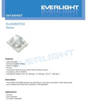
The ELUA2835TG0 series represents a compact, high-performance ultraviolet (UVA) light-emitting diode (LED) solution. This product is engineered for applications requiring ultraviolet light in the 360-410 nanometer (nm) spectrum. The core design philosophy centers on delivering high efficacy and reliable performance within a minimal footprint, making it suitable for integration into space-constrained modern electronic devices.
The primary advantage of this series lies in its combination of a wide viewing angle and low power consumption. The package material is PCT, with a silver coating, contributing to its thermal and electrical performance. It is compliant with major environmental and safety standards, including RoHS, REACH, and halogen-free requirements, ensuring its suitability for global markets.
1.1 Key Features
- Ultraviolet (UVA) emission spectrum.
- Compact surface-mount device (SMD) package measuring 2.8mm x 3.5mm.
- Compliant with RoHS, REACH, and halogen-free directives (Br <900ppm, Cl <900ppm, Br+Cl <1500ppm).
- Lead-free (Pb-free) construction.
- High efficacy and low power consumption.
- Wide viewing angle of 100 degrees.
- Suitable for automated SMT assembly processes.
2. Technical Parameter Deep Dive
This section provides a detailed, objective analysis of the electrical, optical, and thermal parameters specified for the ELUA2835TG0 series. Understanding these parameters is critical for proper circuit design and thermal management.
2.1 Absolute Maximum Ratings
The Absolute Maximum Ratings define the stress limits beyond which permanent damage to the device may occur. These are not recommended operating conditions.
- Maximum DC Forward Current (IF): 70 mA. Exceeding this current can cause catastrophic failure due to overheating or electromigration.
- Maximum Junction Temperature (TJ): 90 °C. The semiconductor die must not exceed this temperature to maintain long-term reliability and prevent performance degradation.
- Operating & Storage Temperature (TOpr, TStg): -40 °C to +85 °C. This range defines the environmental conditions the device can withstand during operation and non-operational storage.
- Thermal Resistance (Rth): 15 °C/W. This parameter indicates how effectively heat travels from the semiconductor junction to the solder pad (or case). A lower value signifies better heat dissipation. For example, at the maximum forward current of 60mA and a typical forward voltage of ~3.5V, the power dissipation is approximately 210mW. This would cause a junction temperature rise of about 3.15°C above the pad temperature (0.21W * 15°C/W).
- Max. ESD Resistance (Human Body Model): 2000V. This specifies the device's sensitivity to electrostatic discharge, a critical factor for handling and assembly procedures.
2.2 Photometric and Electrical Characteristics
The performance of the LED is characterized under specific test conditions, typically at a solder pad temperature of 25°C and a forward current of 60mA.
The datasheet lists four primary product codes within the series, differentiated by their peak wavelength bins:
- ELUA2835TG0-P6070R53040060-VA1D: Peak wavelength 360-370nm.
- ELUA2835TG0-P8090R53040060-VA1D: Peak wavelength 380-390nm.
- ELUA2835TG0-P9000R53040060-VA1D: Peak wavelength 390-400nm.
- ELUA2835TG0-P0010R53040060-VA1D: Peak wavelength 400-410nm.
For all variants, the forward current is specified at 60mA, with a forward voltage range of 3.0V to 4.0V. The radiant flux (optical power output) is binned, with a minimum of 70mW, a typical value of 90mW, and a maximum of 150mW. It is important to note that radiant flux is a measure of total optical power (in watts), not perceived brightness, which is more relevant for visible light.
3. Binning System Explanation
To ensure consistency and allow for selection based on application needs, the LEDs are sorted into performance bins after manufacturing.
3.1 Radiant Flux Bins
LEDs are categorized based on their measured radiant flux at 60mA. The bin codes (R5, R6, R9, S2) define minimum and maximum output ranges, from 70-90mW (R5) up to 130-150mW (S2). Designers can select a bin to guarantee a minimum optical output for their application.
3.2 Peak Wavelength Bins
The emitted ultraviolet light's peak wavelength is binned into 10nm ranges: U36 (360-370nm), U38 (380-390nm), U39 (390-400nm), and U40 (400-410nm). The selection depends on the specific photochemical or fluorescence excitation requirements of the target application. A tolerance of ±1nm is specified for measurement.
3.3 Forward Voltage Bins
Forward voltage (Vf) at 60mA is binned in 0.2V increments, from 3.0-3.2V (Bin 3032) to 3.8-4.0V (Bin 3840). Knowing the Vf bin is important for designing the current-limiting circuitry and predicting power consumption and thermal load. A tolerance of ±2% is applied to these measurements.
4. Performance Curve Analysis
The provided graphs offer crucial insights into the device's behavior under varying operating conditions.
4.1 Relative Spectral Distribution
The graph shows the emission intensity across the wavelength spectrum for the four main wavelength variants (365nm, 385nm, 395nm, 405nm). Each curve has a distinct peak, confirming the binning. The spectral width (full width at half maximum) can be inferred from the graph, which is important for applications requiring specific spectral purity.
4.2 Forward Voltage vs. Forward Current (IV Curve)
This graph illustrates the non-linear relationship between voltage and current. The forward voltage increases with current, and slight variations can be observed between different wavelength chips. This curve is fundamental for selecting an appropriate driver topology (e.g., constant current vs. constant voltage).
4.3 Relative Radiant Flux vs. Forward Current
The optical output increases with drive current but not linearly. The graph shows the relative radiant flux (normalized to the value at a specific current, likely 60mA) rising with current before potentially saturating at higher currents. This informs decisions about driving the LED below its maximum rating to optimize efficacy (light output per electrical watt) or lifespan.
4.4 Thermal Characteristics
Several graphs detail the impact of temperature:
- Relative Radiant Flux vs. Junction Temperature: Shows that optical output decreases as the junction temperature increases. This is a key thermal derating factor.
- Forward Voltage vs. Junction Temperature: Demonstrates that Vf decreases with increasing temperature, which is a characteristic of semiconductor diodes. This can be used for indirect temperature monitoring.
- Peak Wavelength vs. Junction Temperature: Indicates that the peak emission wavelength shifts slightly with temperature, which may be a consideration in precision applications.
- Derating Curve: The most critical graph for reliability. It defines the maximum allowable forward current as a function of the ambient temperature. As ambient temperature rises, the maximum safe current must be reduced to prevent the junction temperature from exceeding its 90°C limit. For example, at an ambient temperature of 85°C, the maximum current is 0mA, meaning the device cannot be operated at that temperature.
5. Mechanical & Packaging Information
5.1 Mechanical Dimensions
The datasheet includes a detailed dimensional drawing of the 2.8mm x 3.5mm package. Key features include the anode and cathode contact pads and a central thermal pad. The thermal pad is noted to be electrically connected to the cathode. Critical tolerances are typically ±0.2mm unless otherwise specified. A crucial handling note warns against applying force to the lens, which could damage the internal structure.
5.2 Polarity Identification
The component drawing clearly marks the anode and cathode pads. Correct polarity is essential during PCB layout and assembly to ensure proper operation.
6. Soldering & Assembly Guidelines
The ELUA2835TG0 is designed for standard surface-mount technology (SMT) processes.
- Reflow Soldering: The device is suitable for reflow soldering. The process must follow standard SMT profiles compatible with the package and PCB materials.
- Reflow Limit: It is recommended not to subject the LED to more than two reflow soldering cycles to minimize thermal stress on the internal components.
- Stress Avoidance: Mechanical stress on the LED body during the heating phase of soldering should be avoided.
- Post-Soldering: Bending the circuit board after soldering is prohibited, as this can crack the solder joints or the LED package itself.
7. Packaging & Ordering Information
7.1 Model Number Nomenclature
The product code follows a detailed structure: ELUA2835TG0-PXXXXYY3040060-VA1D.
- EL: Manufacturer identifier.
- UA: UVA product type.
- 2835: Package dimensions (2.8x3.5mm).
- T: Package material (PCT).
- G: Coating (Ag - Silver).
- 0: Viewing angle (100°).
- PXXXX: Peak wavelength code (e.g., P6070 for 360-370nm).
- YY: Minimum radiant flux bin code (e.g., R5).
- 3040: Forward voltage range (3.0-4.0V).
- 060: Forward current rating (60mA).
- V: Chip type (Vertical).
- A: Chip size (15mil).
- 1: Number of chips (1).
- D: Process type (Dispensing).
7.2 Tape and Reel Packaging
The device is supplied on embossed carrier tape for automated pick-and-place assembly. The datasheet includes dimensions for the carrier tape, which are essential for configuring the SMT equipment's feeder.
8. Application Suggestions
8.1 Typical Application Scenarios
The datasheet lists several applications:
- UV Nail Curing: Used in devices that cure gel nail polish, typically requiring 365nm or 395nm wavelengths.
- UV Counterfeit Detection: Exciting security markings on banknotes, documents, or products that fluoresce under specific UV wavelengths.
- UV Mosquito Traps: Attracting insects, as many are drawn to ultraviolet light in the 365-400nm range.
8.2 Design Considerations
- Driver Circuit: A constant-current driver is strongly recommended to ensure stable optical output and prevent thermal runaway, as the forward voltage has a negative temperature coefficient.
- Thermal Management is paramount. The derating curve must be strictly followed. Adequate PCB copper area (thermal pads) and possible heatsinking are required, especially when operating near maximum ratings or in elevated ambient temperatures.
- Optical Design: The wide 100-degree viewing angle provides broad illumination. For focused beams, secondary optics (lenses) would be necessary.
- ESD Protection: Although rated for 2000V HBM, standard ESD precautions during handling and assembly should be observed.
- Wavelength Selection: Choose the wavelength bin (U36, U38, etc.) based on the absorption spectrum of the target material (e.g., photoinitiator in resin) or the excitation wavelength needed for fluorescence.
9. Technical Comparison & Differentiation
While a direct side-by-side comparison with other products is not provided in the datasheet, key differentiators of the ELUA2835TG0 series can be inferred:
- Package Size: The 2835 footprint is a common industry standard, offering a balance between light output and board space, potentially allowing for easy replacement or upgrade from other 2835 format LEDs.
- Wide Viewing Angle: The 100-degree viewing angle is notably wide for a UVA LED, beneficial for area illumination applications.
- Comprehensive Binning: Detailed binning for flux, wavelength, and voltage allows for precise design and consistent performance in volume production.
- Environmental Compliance: Full compliance with RoHS, REACH, and halogen-free standards is a significant advantage for products targeting international markets with strict regulations.
10. Frequently Asked Questions (Based on Technical Parameters)
Q1: What is the difference between radiant flux (mW) and luminous flux (lm)?
A: Radiant flux measures total optical power in watts. Luminous flux measures perceived brightness by the human eye, weighted by the photopic vision curve. Since UVA is invisible to humans, its performance is correctly specified in radiant flux (mW).
Q2: Can I drive this LED with a 3.3V constant voltage source?
A: It is not recommended. The forward voltage varies from 3.0V to 4.0V (and with temperature). A constant voltage near 3.3V could cause excessive current in a low-Vf device or insufficient current in a high-Vf device. A constant current driver set to 60mA (or lower as per derating) is the correct method.
Q3: Why is the maximum operating ambient temperature 85°C when the junction can go to 90°C?
A: The 85°C ambient limit ensures that under actual operating conditions—with the LED dissipating power (causing a temperature rise from pad to junction)—the junction temperature does not exceed its 90°C maximum. The derating curve graphically defines the safe operating area.
Q4: How do I interpret the \"Relative Radiant Flux vs. Junction Temperature\" graph?
A: The graph shows that output drops as temperature rises. For instance, if the relative flux is 0.8 at 100°C junction temperature, it means the output is only 80% of what it was at the reference temperature (likely 25°C). This must be factored into designs where high ambient temperatures or poor heatsinking are expected.
11. Practical Design Case Study
Scenario: Designing a compact UV nail curing device.
1. Wavelength Selection: Choose the 395nm (U39 bin) or 365nm (U36 bin) variant, as these are common wavelengths for activating photoinitiators in gel polishes.
2. Optical Power Requirement: Determine the required curing intensity and area. Multiple LEDs may be needed. Select the radiant flux bin (e.g., S2 for highest output) to meet the power density requirement.
3. Driver Design: Design a constant-current driver circuit for, say, 50mA per LED (derated from 60mA for longer life and lower thermal load). Calculate the total current needed for the array.
4. Thermal Design: The device will be handheld and may have limited airflow. Use a PCB with large thermal relief pads connected to an internal metal core or a dedicated heatsink. Verify via calculation or simulation that the junction temperature remains below 90°C in the expected worst-case ambient temperature (e.g., 40°C).
5. Layout: Place the LEDs on the PCB with correct polarity. Ensure the thermal pad is properly soldered to a copper pour for heat spreading.
12. Principle of Operation
Ultraviolet LEDs operate on the same fundamental principle as visible LEDs: electroluminescence in a semiconductor material. When a forward voltage is applied across the p-n junction, electrons and holes are injected into the active region. When these charge carriers recombine, they release energy in the form of photons. The wavelength (color) of the emitted light is determined by the bandgap energy of the semiconductor materials used in the active region. For UVA LEDs, materials like aluminum gallium nitride (AlGaN) or indium gallium nitride (InGaN) with specific compositions are engineered to produce photons in the 360-410nm range. The package includes a phosphor-free semiconductor chip, a reflector cup to direct light, and a encapsulating lens that also provides environmental protection.
13. Technology Trends
The field of UV LEDs is advancing rapidly. Key trends include:
- Increased Efficiency: Ongoing research aims to improve the wall-plug efficiency (electrical-to-optical power conversion) of UVA and shorter-wavelength UVB/UVC LEDs, reducing energy consumption and thermal load.
- Higher Power Density: Development of chips and packages capable of handling higher drive currents and dissipating more heat, leading to greater optical output from a single device.
- Wavelength Expansion & Precision: Tighter control over emission wavelengths and the development of LEDs emitting in specific, narrow bands for specialized applications in sensing, medical therapy, and purification.
- Cost Reduction: As manufacturing volumes increase and processes mature, the cost per milliwatt of UV output continues to decrease, making UV LED solutions viable for more consumer and industrial applications previously dominated by mercury-vapor lamps.
- Improved Reliability & Lifetime: Enhancements in materials, packaging, and thermal management are extending the operational lifetime of UV LEDs, a critical factor for commercial and industrial adoption.
LED Specification Terminology
Complete explanation of LED technical terms
Photoelectric Performance
| Term | Unit/Representation | Simple Explanation | Why Important |
|---|---|---|---|
| Luminous Efficacy | lm/W (lumens per watt) | Light output per watt of electricity, higher means more energy efficient. | Directly determines energy efficiency grade and electricity cost. |
| Luminous Flux | lm (lumens) | Total light emitted by source, commonly called "brightness". | Determines if the light is bright enough. |
| Viewing Angle | ° (degrees), e.g., 120° | Angle where light intensity drops to half, determines beam width. | Affects illumination range and uniformity. |
| CCT (Color Temperature) | K (Kelvin), e.g., 2700K/6500K | Warmth/coolness of light, lower values yellowish/warm, higher whitish/cool. | Determines lighting atmosphere and suitable scenarios. |
| CRI / Ra | Unitless, 0–100 | Ability to render object colors accurately, Ra≥80 is good. | Affects color authenticity, used in high-demand places like malls, museums. |
| SDCM | MacAdam ellipse steps, e.g., "5-step" | Color consistency metric, smaller steps mean more consistent color. | Ensures uniform color across same batch of LEDs. |
| Dominant Wavelength | nm (nanometers), e.g., 620nm (red) | Wavelength corresponding to color of colored LEDs. | Determines hue of red, yellow, green monochrome LEDs. |
| Spectral Distribution | Wavelength vs intensity curve | Shows intensity distribution across wavelengths. | Affects color rendering and quality. |
Electrical Parameters
| Term | Symbol | Simple Explanation | Design Considerations |
|---|---|---|---|
| Forward Voltage | Vf | Minimum voltage to turn on LED, like "starting threshold". | Driver voltage must be ≥Vf, voltages add up for series LEDs. |
| Forward Current | If | Current value for normal LED operation. | Usually constant current drive, current determines brightness & lifespan. |
| Max Pulse Current | Ifp | Peak current tolerable for short periods, used for dimming or flashing. | Pulse width & duty cycle must be strictly controlled to avoid damage. |
| Reverse Voltage | Vr | Max reverse voltage LED can withstand, beyond may cause breakdown. | Circuit must prevent reverse connection or voltage spikes. |
| Thermal Resistance | Rth (°C/W) | Resistance to heat transfer from chip to solder, lower is better. | High thermal resistance requires stronger heat dissipation. |
| ESD Immunity | V (HBM), e.g., 1000V | Ability to withstand electrostatic discharge, higher means less vulnerable. | Anti-static measures needed in production, especially for sensitive LEDs. |
Thermal Management & Reliability
| Term | Key Metric | Simple Explanation | Impact |
|---|---|---|---|
| Junction Temperature | Tj (°C) | Actual operating temperature inside LED chip. | Every 10°C reduction may double lifespan; too high causes light decay, color shift. |
| Lumen Depreciation | L70 / L80 (hours) | Time for brightness to drop to 70% or 80% of initial. | Directly defines LED "service life". |
| Lumen Maintenance | % (e.g., 70%) | Percentage of brightness retained after time. | Indicates brightness retention over long-term use. |
| Color Shift | Δu′v′ or MacAdam ellipse | Degree of color change during use. | Affects color consistency in lighting scenes. |
| Thermal Aging | Material degradation | Deterioration due to long-term high temperature. | May cause brightness drop, color change, or open-circuit failure. |
Packaging & Materials
| Term | Common Types | Simple Explanation | Features & Applications |
|---|---|---|---|
| Package Type | EMC, PPA, Ceramic | Housing material protecting chip, providing optical/thermal interface. | EMC: good heat resistance, low cost; Ceramic: better heat dissipation, longer life. |
| Chip Structure | Front, Flip Chip | Chip electrode arrangement. | Flip chip: better heat dissipation, higher efficacy, for high-power. |
| Phosphor Coating | YAG, Silicate, Nitride | Covers blue chip, converts some to yellow/red, mixes to white. | Different phosphors affect efficacy, CCT, and CRI. |
| Lens/Optics | Flat, Microlens, TIR | Optical structure on surface controlling light distribution. | Determines viewing angle and light distribution curve. |
Quality Control & Binning
| Term | Binning Content | Simple Explanation | Purpose |
|---|---|---|---|
| Luminous Flux Bin | Code e.g., 2G, 2H | Grouped by brightness, each group has min/max lumen values. | Ensures uniform brightness in same batch. |
| Voltage Bin | Code e.g., 6W, 6X | Grouped by forward voltage range. | Facilitates driver matching, improves system efficiency. |
| Color Bin | 5-step MacAdam ellipse | Grouped by color coordinates, ensuring tight range. | Guarantees color consistency, avoids uneven color within fixture. |
| CCT Bin | 2700K, 3000K etc. | Grouped by CCT, each has corresponding coordinate range. | Meets different scene CCT requirements. |
Testing & Certification
| Term | Standard/Test | Simple Explanation | Significance |
|---|---|---|---|
| LM-80 | Lumen maintenance test | Long-term lighting at constant temperature, recording brightness decay. | Used to estimate LED life (with TM-21). |
| TM-21 | Life estimation standard | Estimates life under actual conditions based on LM-80 data. | Provides scientific life prediction. |
| IESNA | Illuminating Engineering Society | Covers optical, electrical, thermal test methods. | Industry-recognized test basis. |
| RoHS / REACH | Environmental certification | Ensures no harmful substances (lead, mercury). | Market access requirement internationally. |
| ENERGY STAR / DLC | Energy efficiency certification | Energy efficiency and performance certification for lighting. | Used in government procurement, subsidy programs, enhances competitiveness. |