Teburin abubuwan ciki
- 1. Bayanin samfur
- 1.1 Core Advantages and Target Market
- 2. In-depth Technical Parameter Analysis
- 2.1 Absolute Maximum Ratings
- 2.2 Electrical Characteristics
- 2.3 Transmission Characteristics
- 3. Grading System Description
- 4. Performance Curve Analysis
- 5. Mechanical and Packaging Information
- 6. Soldering and Assembly Guide
- 7. Ordering and Packaging Information
- 8. Application Recommendations
- 8.1 Typical Application Circuit
- 8.2 Design Considerations
- 9. Technical Comparison and Differentiation
- 10. Frequently Asked Questions (FAQ)
- 11. Practical Design Case Study
- 12. Working Principles
- 13. Technology Trends
- Detailed Explanation of LED Specification Terminology
- I. Core Photoelectric Performance Indicators
- II. Electrical Parameters
- III. Thermal Management and Reliability
- IV. Packaging and Materials
- V. Quality Control and Binning
- VI. Testing and Certification
1. Bayanin samfur
The CNY64S series represents a class of high-performance optocouplers (optical isolators), specifically designed for applications requiring robust electrical isolation and reliable signal transmission. The core of the device consists of an infrared gallium arsenide (GaAs) light-emitting diode (LED) optically coupled to a silicon NPN phototransistor. This configuration allows for the transfer of electrical signals between two circuits while maintaining a high degree of electrical isolation, preventing damage to sensitive components from ground loops, noise transmission, and high-voltage surges.
The primary design objectives of the CNY64S series are to provideReinforced Safety IsolationThis is achieved by combining sufficient creepage distance and electrical clearance (ensured by encapsulation with insulation penetration thickness ≥3mm) along with high dielectric strength material. The device employs a compact 4-pin dual in-line package (DIP), a through-hole mounting method that provides mechanical stability and facilitates manual or wave soldering processes. This series is characterized by its extremely high isolation voltage ratings, making it suitable for industrial, power supply, and medical equipment where user safety and system integrity are paramount.
1.1 Core Advantages and Target Market
The key advantages of the CNY64S optocoupler stem from its safety-oriented design and reliable performance parameters.
- Superior Isolation Performance:The standard version offers a maximum transient isolation voltage (VIOTM) peak of 8200V, while the VDE-certified "-V" model provides a peak of 10000V, delivering exceptional protection against high-voltage transient events. The rated repetitive peak isolation voltage (VIORM) is 2200V.
- High Voltage Capability:The minimum collector-emitter breakdown voltage (BVCEO) of the output phototransistor is 80V, enabling it to interface directly with higher voltage circuits in many applications without requiring additional buffering.
- Safety Certifications:The device is approved by major international safety standard bodies, including CUL, VDE, and FIMKO. The VDE certification specifically attests to its compliance with DIN EN 60747-5-5 standards forReinforced IsolationRequirement, this is a critical requirement for safety-critical applications.
- Environmental Compliance:Manufactured using lead-free (Pb-free) processes and compliant with the RoHS (Restriction of Hazardous Substances) directive.
- Wide Operating Range:Capable of reliable operation over an extended temperature range from -55°C to +85°C.
The target markets for CNY64S includeSwitch-Mode Power Supply (SMPS)feedback loop isolation design,Industrial AutomationSystems (PLC I/O, motor drives), requiring patient isolationMedical Equipment、TelecommunicationsEquipment, and any signals that must safely cross different voltage domains or safety boundariesMicroprocessor-based systems。
2. In-depth Technical Parameter Analysis
A fahimtar cikakken sigogi na lantarki da na gani yana da mahimmanci don ƙirar da'ira daidai da tabbatar da dogon aminci.
2.1 Absolute Maximum Ratings
Waɗannan ƙididdiga suna ayyana iyakokin damuwa waɗanda zasu iya haifar da lalacewar na'ura na dindindin. Ba a amfani da su a cikin yanayin aiki na yau da kullun ba.
- Shigarwa (LED):Matsakaicin ci gaba na yanzu (IF) shine 75 mA. An yarda da gajeriyar ƙarfin kololuwa na 1.5A (IFM). The absolute maximum reverse voltage (VR) is only 5V, highlighting the LED's sensitivity to reverse bias. Exceeding this value will quickly lead to LED performance degradation. The input power dissipation (PD) must not exceed 120 mW.
- Output (Phototransistor):Maximum continuous collector current (IC) is 50 mA. The collector power dissipation (PC) is limited to 150 mW. The collector-emitter voltage (VCEO) must be kept below 80V, and the emitter-collector voltage (VECO) must be kept below 7V.
- Device Limits:Total device power consumption (Ptot) is 250 mW. Isolation voltage (Viso) is tested at 8200 VRMSfor one minute under controlled humidity (40-60% RH).
2.2 Electrical Characteristics
These parameters are guaranteed under specified test conditions and define the performance of the device.
- Input Characteristics:At a forward current of 50mA, the LED forward voltage (VF) has a typical value of 1.6V and a maximum of 2.0V. This is important for calculating the current-limiting resistor value. The reverse leakage current (IR)非常低(5V时<10 µA)。
- Output Characteristics:Dark current (ICEO), which is the leakage current of the phototransistor when the LED is off, is a maximum of 200 nA at VCE=20V. This parameter is crucial for determining the signal integrity and noise floor in the off state. When the transistor is fully on, VCE(sat)) is a maximum of 0.3V (IF=10mA, IC=1mA), indicating its good switching performance.
- Isolation Characteristics:Coupling Capacitance (CIO) The typical value is very low, at 0.3 pF, which minimizes capacitive coupling of high-frequency noise through the isolation barrier. The isolation resistance (RIO) is a minimum of 1011Ω (100 GΩ) at 500V DC, representing excellent DC insulation performance.
2.3 Transmission Characteristics
This is the core of the optocoupler's function, defining the relationship between the input current and the output current.
- Current Transfer Ratio (CTR):This is the ratio of the output collector current (IC) to the input LED forward current (IF), expressed as a percentage (CTR = IC/ IF* 100%). The CNY64S series offers three CTR grades or "bins":
- CNY64S:CTR ranges from 50% to 300%.
- CNY64SA:CTR ranges from 63% to 125%.
- CNY64SB:CTR range from 100% to 200%.
CTR is measured under standard conditions (IF= 5mA, VCE= 5V). Selecting the appropriate CTR grade allows designers to optimize for gain, power efficiency, or switching speed. Devices with higher CTR require less LED drive current to achieve the same output current, thereby improving efficiency, but their dynamic characteristics may differ slightly.
- Switching speed:Dynamic performance is determined by the turn-on time (ton), turn-off time (toff), rise time (tr) and fall time (tf) characterize. For CNY64S, under the test conditions of VCC=5V, IC=5mA, RL=100Ω, the maximum value for all timing parameters is 18 µs, while the typical values are much faster (e.g., ton~6µs, toff~7µs). These speeds are suitable for digital signal isolation and lower frequency PWM signals, but not for very high-speed data communication.
3. Grading System Description
The CNY64S series employs a simple grading system based solely onCurrent Transfer Ratio (CTR). In this specific device series, there is no grading for wavelength or forward voltage, as it uses a standard infrared LED.
The model number indicates the CTR grade:
- Base ModelCNY64Sindicates the standard wide-range CTR bin (50-300%).
- Suffix-A(e.g., CNY64SA) specifies a tighter CTR grade with a range of 63-125%.
- Suffix-B(e.g., CNY64SB) specifies a tighter CTR grade with a range of 100-200%.
- Optional suffix-VIndicates that the component has received VDE safety certification for reinforced isolation.
This grading allows system designers to select devices with guaranteed minimum and maximum CTR values. For example, in linear analog feedback applications, tighter CTR grades (A or B) ensure more consistent gain across different devices, thereby improving production yield and performance consistency. For simple digital switching isolation, the standard grade may be entirely sufficient and more cost-effective.
4. Performance Curve Analysis
Although the provided PDF excerpt mentions "typical performance curves" but does not show them, typical curves for optocouplers like the CNY64S would include the following, which are crucial for design:
- CTR vs. Forward Current (IF):This curve shows how CTR varies with drive current. Typically, CTR is highest at moderate forward currents (e.g., 5-10mA) and may decrease at very low or very high currents. This helps in selecting the operating point for optimal efficiency and linearity.
- CTR vs. Temperature:The CTR of an optocoupler typically has a negative temperature coefficient; it decreases as the ambient temperature rises. Understanding this derating is crucial for designing systems that must operate reliably across the full -55°C to +85°C range.
- Forward Voltage (VF) vs. Forward Current (IF):The standard IV curve for the infrared LED, used for thermal management and driver design.
- Switching Time vs. Load Resistance (RL):Switching speed (ton, toff) depends heavily on the load resistor connected to the phototransistor collector. A smaller RLgenerally provides faster switching speed, at the cost of higher power consumption and lower output voltage swing.
The test circuit for switching time (Figure 10 in the PDF) shows a standard configuration: a pulse drives the LED through a current-limiting resistor (RIN), and the phototransistor output is monitored across a load resistor (RL) connected to the supply voltage (VCC). The waveform defines timing parameters between the 10% and 90% points of the input and output pulses.
5. Mechanical and Packaging Information
The CNY64S uses a 4-pin DIP (Dual In-line Package). The key mechanical characteristic for safety isthe insulation penetration distance, which is guaranteed to be ≥3mm. This physical isolation between the input side (pins 1 and 2) and the output side (pins 3 and 4) of the package is a fundamental requirement for achieving reinforced isolation grade under high voltage.
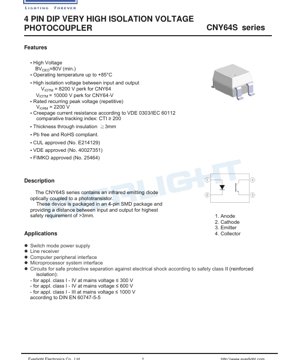
Pin Definition:
- Infrared LED Anode
- Infrared LED Cathode
- Phototransistor Emitter
- Phototransistor Collector
The package drawing (implied in the PDF) will provide precise dimensions for PCB pad planning, including pin pitch, body width, and overall height. It also provides a recommended surface mount pad layout (possibly for DIP packages with through-hole mounting but pins formed for surface mounting) to ensure reliable solder joint connections and adequate mechanical strength during assembly.
6. Soldering and Assembly Guide
This device can withstand a maximum soldering temperature of 260°C measured 2mm from the package body for a duration of less than 10 seconds. This is compatible with standard lead-free reflow and wave soldering processes. Care must be taken to avoid excessive thermal stress, which could damage internal wire bonds or plastic package material, potentially compromising isolation integrity. Standard industry practices for handling moisture-sensitive devices (if applicable) should be followed. The storage temperature range is -55°C to +100°C.
7. Ordering and Packaging Information
The model structure is as follows:CNY64SX-V
- CNY64S:Series base model.
- X:CTR rating options: 'A', 'B', or blank (standard rating).
- -V:Optional suffix, indicating VDE safety certification.
Packaging options:
- CNY64S / CNY64S-V:Tube packaging, 60 pieces per tube.
- CNY64S(TA):Tube packaging, 500 pieces per tube (possibly a bulk packaging option).
Device marking:The top of the package is marked with several lines of text:
- EL:Manufacturer code.
- CNY64:Modeli ya msingi.
- R:Herufi moja inayoonyesha kiwango cha CTR (k.m. 'A' au 'B').
- Y:Nambari ya tarakimu moja inayoonyesha mwaka wa utengenezaji.
- WW:Nambari ya tarakimu mbili inayoonyesha wiki ya utengenezaji.
- V:Optional marking indicating VDE certification.
8. Application Recommendations
8.1 Typical Application Circuit
CNY64S is versatile and can be used in several key configurations:
- Digital Signal Isolation:The simplest use case. A digital signal drives the LED through a current-limiting resistor. The phototransistor is connected as a switch, with a pull-up resistor connected to VCC, reconstructing the inverted logic signal on the isolated side. The switching speed (max. 18µs) supports data rates up to tens of kHz.
- Switched-Mode Power Supply (SMPS) Feedback:One key application. Optocouplers are used to transfer the error voltage from the secondary (output) side of the power supply back to the PWM controller on the primary side, while maintaining the isolation barrier. The linearity and temperature stability of the CTR are very important here. High isolation voltage is crucial for the safety of offline power supplies.
- Microprocessor System Interface:Isolating digital I/O lines between noisy industrial environments (e.g., 24V PLC inputs) and sensitive microprocessors. A BV of 80VCEOprovides a good margin for voltage spikes.
8.2 Design Considerations
- LED Current Limiting:Always use a series resistor to set the LED forward current (IF). Based on the supply voltage (Vsupply), the required IFand the LED's VF(Use the maximum value in worst-case design) Calculate the resistor value: R = (Vsupply- VF) / IF. Do not exceed the absolute maximum I of 75mA.F。
- Phototransistor Bias:The load resistor (RL) on the collector determines the output voltage swing, switching speed, and power consumption. A smaller RLprovides faster speed but lower gain and higher current. Ensure the voltage across the phototransistor (VCE) In the off state, it does not exceed 80V.
- CTR Degradation:The CTR of an optocoupler gradually decreases over time, especially when operating at high junction temperatures and high forward currents. For long-life designs, the operating IFshould be derated and sufficient thermal management ensured. Select a device with an initial CTR significantly higher than the minimum required by the circuit at the end of its life.
- Noise Immunity:Low coupling capacitance (0.3 pF) provides good high-frequency common-mode noise rejection. For extremely noisy environments, consider adding a small bypass capacitor (e.g., 0.1µF) near the device's input and/or output pins to filter out high-frequency spikes.
9. Technical Comparison and Differentiation
Compared to those with lower isolation ratings (e.g., 2500VRMSau 5000VRMS) ya daidaitaccen 4-pin photodiode coupler, babban bambancin CNY64S shine8200VRMS/10000V kololuwar keɓewada na yau da kullunƙarfafa keɓewa takaddun shaida(VDE). Wannan ya sa ba kawai mai keɓewa sigina ba ne, amma kuma abu ne na aminci da aka tabbatar. Idan aka kwatanta da saurin mai keɓewa na dijital (yana amfani da capacitor ko magnetic coupling), CNY64S yana da sauri, amma yana ba da ƙarin ƙarfin keɓewa da ƙarfin dV/dt na wucin gadi, kuma yawanci yana da ƙarancin farashi. Haɗin ƙimar transistor na fitarwa na 80V, zaɓin CTR mai yawa, da takaddun shaida na aminci, sun haifar da ƙimar ƙima mai ƙarfi ga aikace-aikacen masana'antu da wutar lantarki masu mahimmanci amma masu rauni.
10. Frequently Asked Questions (FAQ)
Q1: Menene bambanci tsakanin daidaitaccen CNY64S da CNY64S-V?
A1: The "-V" model has undergone additional testing and certification by VDE according to a specific safety standard (DIN EN 60747-5-5) for reinforced isolation. It has a higher transient isolation voltage rating (10000V peak vs. 8200V peak). The -V version is required for applications needing formal safety agency recognition.
Q2: How to choose between CTR grades (Standard, A, B)?
A2: If your circuit design can tolerate large gain variations (e.g., digital switching with ample margin), the Standard grade is sufficient. If you need more consistent performance between different devices, especially in analog feedback loops or circuits where a specific minimum CTR is critical to functionality, choose grade A or B. Grade B guarantees a higher minimum CTR (100%).
Q3: Can I use it for isolating AC mains voltage signals?
A3: Yes, but with important caveats. The device is rated for reinforced isolation of mains voltages up to specific limits, depending on the application category (e.g., up to 600V for Categories I-IV). You must ensure that the creepage and clearance distances on the PCB around the device also meet the relevant safety standards for your working voltage. The optocoupler itself is only part of the isolation system.
Q4: Why is the reverse voltage rating of the LED so low (5V)?
A4: The infrared LED is a semiconductor diode with a relatively low reverse breakdown voltage. Applying even a small reverse voltage exceeding the rating can cause avalanche breakdown and immediate damage. Always ensure the drive circuit prevents reverse bias, or if reverse voltage is possible, connect a protection diode in parallel across the LED (cathode to anode).
11. Practical Design Case Study
Scenario:Isolate the 5V digital signal from the microcontroller to control a 24V relay in an industrial cabinet. The environment has electrical noise, requiring functional isolation to prevent ground loop interference with the microcontroller.
Design Steps:
- Component Selection:Select CNY64SB to guarantee a minimum CTR of 100%, ensuring robust driving capability even after aging.
- LED Driver:The microcontroller pin (5V output) drives the LED. Target IF= 10mA for good speed and margin. Use VF(max)= 2.0V, Rlimit= (5V - 2.0V) / 0.01A = 300Ω. Use a standard 330Ω resistor, yielding IF≈ 9mA.
- Output circuit:The relay coil (24V, 100Ω coil resistance) is connected between the 24V supply and the phototransistor's collector. The emitter is grounded. When the LED is on, the phototransistor saturates, pulling the collector low and thus energizing the relay. A flyback diode must be placed across the relay coil to suppress voltage spikes when the transistor turns off. The 0.3V VCE(sat)is negligible. The 80V BVCEOProvides ample protection for the inductive kickback spike that the diode fails to fully clamp.
- PCB layout:Maintain a creepage distance of ≥3mm on the PCB between the input-side traces (microcontroller, resistor) and output-side traces (24V, relay) to extend the internal isolation of the device. Place bypass capacitors (0.1µF) near the power pins on both sides of the device.
This simple and robust circuit reliably isolates the control logic from the power stage by leveraging the key parameters of the CNY64S.
12. Working Principles
The CNY64S is based on theelectro-optical-electrical conversionprinciple. The current applied to the input side flows through the infrared LED, causing it to emit photons with a wavelength typically around 940nm. This light passes through the transparent insulating gap within the plastic package. On the output side, the light irradiates the base region of the silicon NPN phototransistor, generating electron-hole pairs. This photogenerated current acts as the base current, which is then amplified by the transistor's gain (hFE)放大,产生大得多的集电极电流。关键点在于,输入和输出之间的唯一连接是光束;没有电导体,从而提供了电气隔离。隔离程度由光路的物理距离和中间材料的介电特性决定。
13. Technology Trends
Optocoupler technology continues to evolve. While the fundamental principles remain unchanged, trends include:
- Higher Integration:Integrating optocouplers with additional circuits such as Schmitt triggers, gate drivers, or I²C isolators into a single package.
- Faster Speeds:Developing faster phototransistors and integrated designs for digital isolation competing in the Mbps range.
- Enhanced Reliability and Miniaturization:Improving LED efficiency and packaging materials to extend lifespan, reduce CTR degradation, and enable the use of smaller surface-mount packages (e.g., SO-4, SO-6) while maintaining high isolation ratings.
- Focus on Safety Standards:Growing demand for components with pre-certified reinforced isolation to simplify end-product compliance with stringent global safety regulations for medical, automotive, and industrial equipment.
Detailed Explanation of LED Specification Terminology
Complete Explanation of LED Technical Terminology
I. Core Photoelectric Performance Indicators
| Terminology | Unit/Penyajian | Penjelasan Populer | Mengapa Penting |
|---|---|---|---|
| Efikasi Cahaya (Luminous Efficacy) | lm/W (lumen per watt) | Fluks cahaya yang dihasilkan per watt daya listrik, semakin tinggi semakin hemat energi. | Directly determines the energy efficiency rating and electricity cost of the lighting fixture. |
| Luminous Flux | lm (lumen) | The total amount of light emitted by a light source, commonly referred to as "brightness". | Determines whether the lighting fixture is bright enough. |
| Viewing Angle | °, e.g., 120° | The angle at which light intensity drops to half, determining the beam width. | Affects the illumination range and uniformity. |
| CCT | K, e.g., 2700K/6500K | The color warmth of light; lower values are yellowish/warm, higher values are whitish/cool. | Determines the lighting atmosphere and suitable application scenarios. |
| Color Rendering Index (CRI / Ra) | Unitless, 0–100 | The ability of a light source to reproduce an object's true colors, Ra≥80 is preferred. | Affects color authenticity, used in high-demand places like shopping malls, art galleries, etc. |
| Color Tolerance (SDCM) | MacAdam ellipse steps, e.g., "5-step" | A quantitative metric for color consistency; a smaller step number indicates better color consistency. | Ensures no color variation among luminaires from the same batch. |
| Dominant Wavelength | nm (nanometer), e.g., 620nm (red) | The wavelength value corresponding to the color of a colored LED. | Determines the hue of monochromatic LEDs such as red, yellow, and green. |
| Spectral Distribution | Wavelength vs. Intensity curve | Shows the intensity distribution of light emitted by an LED across various wavelengths. | Affects color rendering and color quality. |
II. Electrical Parameters
| Terminology | Symbol | Penjelasan Populer | Design Considerations |
|---|---|---|---|
| Forward Voltage | Vf | The minimum voltage required to turn on an LED, similar to a "starting threshold". | The driving power supply voltage must be ≥ Vf; voltages add up when multiple LEDs are connected in series. |
| Forward Current | If | The current value that enables the LED to emit light normally. | Constant current drive is commonly used; the current determines brightness and lifespan. |
| Maximum Pulse Current | Ifp | Peak current that can be sustained for a short period, used for dimming or flashing. | Pulse width and duty cycle must be strictly controlled, otherwise overheating damage may occur. |
| Reverse Voltage | Vr | The maximum reverse voltage that an LED can withstand; exceeding it may cause breakdown. | The circuit must be protected against reverse connection or voltage surges. |
| Thermal Resistance | Rth (°C/W) | The resistance to heat flow from the chip to the solder joint; a lower value indicates better heat dissipation. | A high thermal resistance requires a more robust heat dissipation design; otherwise, the junction temperature will increase. |
| ESD Immunity | V (HBM), e.g., 1000V | Anti-static strike capability, the higher the value, the less susceptible to damage from static electricity. | Anti-static measures must be implemented during production, especially for high-sensitivity LEDs. |
III. Thermal Management and Reliability
| Terminology | Key Indicators | Penjelasan Populer | Impact |
|---|---|---|---|
| Junction Temperature | Tj (°C) | The actual operating temperature inside the LED chip. | For every 10°C reduction, lifespan may double; excessively high temperature leads to lumen depreciation and color shift. |
| Lumen Depreciation | L70 / L80 (hours) | The time required for brightness to drop to 70% or 80% of its initial value. | Ayyana kai tsaye "rayuwar aiki" na LED. |
| Lumen Maintenance | % (misali 70%) | Kashi na hasken da ya rage bayan amfani na wani lokaci. | Yana nuna ikon riƙe haske bayan amfani na dogon lokaci. |
| Color Shift | Δu′v′ or MacAdam Ellipse | The degree of color change during use. | Affects the color consistency of the lighting scene. |
| Thermal Aging | Degradation of material performance. | Deterioration of packaging materials due to prolonged high temperatures. | May lead to decreased brightness, color shift, or open-circuit failure. |
IV. Packaging and Materials
| Terminology | Common Types | Penjelasan Populer | Characteristics and Applications |
|---|---|---|---|
| Packaging Types | EMC, PPA, Ceramic | The housing material that protects the chip and provides optical and thermal interfaces. | EMC offers good heat resistance and low cost; ceramics provide superior heat dissipation and long lifespan. |
| Chip Structure | Front-side, Flip Chip | The arrangement method of chip electrodes. | Flip Chip offers better heat dissipation and higher luminous efficacy, suitable for high-power applications. |
| Phosphor coating | YAG, silicate, nitride | Coated on the blue LED chip, partially converted to yellow/red light, mixed to form white light. | Different phosphors affect light efficiency, color temperature, and color rendering. |
| Lens/optical design | Flat, microlens, total internal reflection | Optical structure on the packaging surface, controlling light distribution. | Determines the emission angle and light distribution curve. |
V. Quality Control and Binning
| Terminology | Binning Content | Penjelasan Populer | Purpose |
|---|---|---|---|
| Luminous Flux Binning | Codes such as 2G, 2H | Grouped by brightness level, each group has a minimum/maximum lumen value. | Ensure consistent brightness within the same production batch. |
| Voltage binning | Codes such as 6W, 6X | Grouped by forward voltage range. | Facilitates driver matching and improves system efficiency. |
| Color binning. | 5-step MacAdam ellipse. | Group by color coordinates to ensure colors fall within a very narrow range. | Ensures color consistency and avoids color variation within the same luminaire. |
| Color temperature binning. | 2700K, 3000K, etc. | Group by color temperature, each group has a corresponding coordinate range. | Meet the color temperature requirements of different scenarios. |
VI. Testing and Certification
| Terminology | Standard/Test | Penjelasan Populer | Significance |
|---|---|---|---|
| LM-80 | Lumen Maintenance Test | Long-term operation under constant temperature conditions, recording data on luminous flux depreciation. | Used to estimate LED lifetime (in conjunction with TM-21). |
| TM-21 | Lifetime Projection Standard | Projecting lifespan under actual use conditions based on LM-80 data. | Providing scientific life prediction. |
| IESNA Standard | Illuminating Engineering Society Standard | Covers optical, electrical, and thermal testing methods. | Industry-recognized testing basis. |
| RoHS / REACH | Environmental certification | Ensure the product does not contain harmful substances (such as lead, mercury). | Entry requirements for the international market. |
| ENERGY STAR / DLC | Energy efficiency certification | Energy efficiency and performance certification for lighting products. | Commonly used in government procurement and subsidy programs to enhance market competitiveness. |