İçindekiler
- 1. Ürün Genel Bakışı
- 2. Teknik Parametrelerin Detaylı Açıklaması
- 2.1 Mutlak Maksimum Değerler
- 2.2 Optoelektronik Özellikler
- 3. Performans Eğrisi Analizi
- 3.1 Spektral Duyarlılık
- 3.2 Karanlık Akım ile Ortam Sıcaklığı İlişkisi
- 3.3 Ters Yönlü Fotoakım ile Işınım Şiddeti Arasındaki İlişki
- 3.4 Uç Kapasitansı ile Ters Gerilim Arasındaki İlişki
- 3.5 Tepki Süresi ile Yük Direnci İlişkisi
- 3.6 Güç Tüketimi ile Ortam Sıcaklığı İlişkisi
- 4. Mekanik ve Paketleme Bilgileri
- 4.1 Paket Boyutları
- 4.2 Polarite Tanımlama
- 5. Lehimleme ve Montaj Kılavuzu
- 6. Paketleme ve Sipariş Bilgileri
- 6.1 Paketleme Özellikleri
- 6.2 Etiket Özellikleri
- 7. Uygulama Önerileri
- 7.1 Tipik Uygulama Senaryoları
- 7.2 Tasarım Değerlendirmeleri
- 8. Teknik Karşılaştırma ve Farklılaşma
- 9. Sıkça Sorulan Sorular (Teknik Parametrelere Dayalı)
- 10. Gerçek Tasarım ve Kullanım Örnekleri
- 11. Çalışma Prensibi Özeti
- 12. Teknoloji Trendleri ve Arka Plan
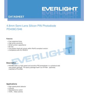
1. Ürün Genel Bakışı
PD438C/S46, hızlı tepki süresi ve kızılötesi ışığa yüksek hassasiyet gerektiren uygulamalar için tasarlanmış yüksek performanslı bir silikon PIN fotodiyottur. Kompakt, silindirik, yandan bakışlı plastik bir paketle sunulur ve çapı 4.8 mm'dir. Cihazın önemli bir özelliği, epoksi paketlemesinin entegre bir kızılötesi filtre görevi görmesidir. Spektral karakteristiği, yaygın kızılötesi vericilerle uyumludur ve istenmeyen görünür ışığı filtreleyerek kızılötesi algılama sistemlerindeki performansını artırır.
Bu fotodiyot, hızlı tepki süresi, yüksek ışık hassasiyeti ve düşük bağlantı kapasitansı ile karakterize edilir ve bu da onu yüksek hızlı optik algılama için uygun kılar. Kurşunsuz malzemeler kullanılarak üretilmiştir ve ilgili çevre düzenlemelerine uygundur.
2. Teknik Parametrelerin Detaylı Açıklaması
2.1 Mutlak Maksimum Değerler
Bu cihaz, belirtilen limitler dahilinde güvenilir çalışacak şekilde tasarlanmıştır. Bu değerlerin aşılması kalıcı hasara neden olabilir.
- Ters Gerilim (VR):32 V - Fotodiyot terminalleri arasına uygulanabilecek maksimum ters öngerilim voltajı.
- Güç Tüketimi (Pd):150 mW - Belirtilen koşullar altında, cihazın başlıca ısı şeklinde dağıtabileceği maksimum güç.
- Çalışma Sıcaklığı (Topr):-40°C ila +85°C - Cihazın yayınlanan özelliklerini karşıladığının garanti edildiği ortam sıcaklığı aralığı.
- Depolama Sıcaklığı (Tstg):-40°C ila +100°C - Cihaz güç verilmeden güvenle depolanabilecek sıcaklık aralığı.
- Lehimleme sıcaklığı (Tsol):260°C, süresi 5 saniyeyi aşmamak üzere, bu tipik kurşunsuz geri akış lehimleme proses gereksinimlerine uygundur.
2.2 Optoelektronik Özellikler
Bu parametreler ortam sıcaklığında (Ta) 25°C'de ölçülmüştür, fotodiyodun temel performansını tanımlar.
- Spektral bant genişliği (λ0.5):840 nm ila 1100 nm. Bu, fotodiyodun duyarlılığının en az tepe değerinin yarısı olduğu dalga boyu aralığını tanımlar. Esas olarak yakın kızılötesi bölgedeki ışığa duyarlıdır.
- Tepe hassasiyet dalga boyu (λp):940 nm (tipik). Fotodiyodun en hassas olduğu ışık dalga boyu. Bu, birçok kızılötesi LED'in yaygın emisyon dalga boyu ile eşleşir.
- Açık devre voltajı (VOC):0.35 V (tipik değer), 940 nm dalga boyunda, 5 mW/cm² ışınım (E) altında ölçülmüştür.eBu, fotodiyodun harici bir yük olmadan ürettiği voltajdır.
- Kısa devre akımı (ISC):18 µA (tipik), Ee= 1 mW/cm², λp=940nm koşullarında. Bu, çıkış kısa devre yapıldığındaki fotoakımdır.
- Ters fotoakım (IL):18 µA (tipik, minimum 10.2 µA), Ee= 1 mW/cm², λp=940nm ve ters öngerilim voltajı (VR) 5V koşullarında. Bu, fotokondüktif moddaki ana çalışma parametresidir.
- Karanlık akım (Id):5 nA (tipik, maksimum 30 nA), VR= 10V ve tamamen karanlık koşullarında. Bu, hiç ışık olmadığında bile akan küçük sızıntı akımıdır ve sinyal-gürültü oranı için kritik bir parametredir.
- Ters kırılma gerilimi (BVR):Minimum 32V, tipik 170V, ters akım 100 µA iken ölçülür. Bu, bağlantının kırılma gerilimini ifade eder.
- Toplam kapasitans (Ct):18 pF (tipik), VR= 3V ve test frekansı 1 MHz koşullarında. Düşük kapasitans daha hızlı tepki süresi sağlar.
- Yükselme/alçalma süresi (tr/tf):50 ns / 50 ns (tipik), VR= 10V ve yük direnci (RL) 1 kΩ koşullarında. Bu, fotodiyodun ışık darbelerine tepki hızını belirler.
Kritik parametrelerin toleransları şu şekilde belirlenmiştir: Işık şiddeti ±%10, ana dalga boyu ±1nm, ileri voltaj ±0.1V.
3. Performans Eğrisi Analizi
Veri sayfası, farklı koşullar altındaki performansı gösteren birkaç karakteristik eğri sağlar. Bunlar tasarım mühendisleri için çok önemlidir.
3.1 Spektral Duyarlılık
Göreceli duyarlılığı dalga boyuna karşı çizen bir eğri. Yaklaşık 940 nm'deki tepe duyarlılığını doğrular ve spektral tepkinin 840-1100 nm aralığının sınırlarında kademeli olarak düştüğünü gösterir. Entegre epoksi lens, hedef kızılötesi bandın dışındaki tepkiyi zayıflatarak bir filtre görevi görür.
3.2 Karanlık Akım ile Ortam Sıcaklığı İlişkisi
Bu eğri tipik olarak karanlık akımın (Id) sıcaklık arttıkça üstel olarak arttığını gösterir. Bu ilişkiyi anlamak, geniş bir sıcaklık aralığında çalışan uygulamalar için hayati önem taşır, çünkü tespit edilebilir ışığın alt sınırını (gürültü tabanını) tanımlar.
3.3 Ters Fotoakım ile Işınım Şiddeti (Ee)
) İlişkiLBu grafik, üretilen fotoelektrik akımın (I
) ile gelen ışık güç yoğunluğu arasındaki doğrusal ilişkiyi göstermektedir. Belirtilen koşullar altında, fotodiyot yüksek derecede doğrusal bir bölgede çalışır, bu da analog optik ölçüm uygulamaları için çok önemlidir.
3.4 Uç Kapasitansı ile Ters Gerilim Arasındaki İlişkitBağlantı kapasitansı (C
), ters öngerilim voltajının artmasıyla azalır. Bu, PN bağlantısının temel bir özelliğidir. Tasarımcılar, kapasitansı düşürmek, böylece bant genişliğini ve tepki hızını artırmak için daha yüksek öngerilim voltajı kullanabilir; bunun bedeli karanlık akımda hafif bir artıştır.
3.5 Tepki Süresi ile Yük Direnci İlişkisiLBu eğri, yükselme/düşme sürelerinin harici yük direnci (RL) değerinin etkisi. Daha küçük R
genellikle daha hızlı bir tepkiye yol açar, ancak daha küçük bir çıkış voltajı salınımı üretir. Bu grafik, devre tasarımında hız ve genlik arasındaki dengeyi optimize etmeye yardımcı olur.
3.6 Güç Tüketimi ile Ortam Sıcaklığı İlişkisi
Ortam sıcaklığı arttıkça maksimum izin verilen güç tüketiminin nasıl düşürüldüğünü (derating) açıklar. Sıcaklık 25°C'nin üzerine çıktığında, cihaz tüm 150mW'ı dağıtamaz; maksimum güç, maksimum jonksiyon sıcaklığına ulaşıldığında doğrusal olarak sıfıra düşürülmelidir.
4. Mekanik ve Paketleme Bilgileri
4.1 Paket Boyutları
PD438C/S46, nominal çapı 4.8 mm olan silindirik yandan görünümlü plastik paket kullanır. Boyut diyagramı, gövde çapını, uzunluğu, bacak aralığını ve bacak çapını belirtir. Önemli bir not, çizimde aksi belirtilmedikçe tüm boyut toleranslarının ±0.25 mm olduğunu belirtir. Yandan görünüm konfigürasyonu, optik yolun PCB yüzeyine paralel olduğu uygulamalar için idealdir.
4.2 Polarite Tanımlama
Polarite genellikle paket üzerinde veya çizimlerde belirtilir. Fotodiyotlar ters öngerilimli (fotoiletken mod) çalıştırıldığında, katot genellikle pozitif besleme voltajına, anot ise devre toprağına veya transimpedans yükseltecinin girişine bağlanır. Doğru polarite, düzgün çalışma için çok önemlidir.
5. Lehimleme ve Montaj Kılavuzu
- Bu cihaz, standart yüzey montajı üretim süreçlerine uygundur.Reflow lehimleme:
- Önerilen maksimum lehimleme sıcaklığı 260°C'dir. Cihaz bacaklarının bu tepe sıcaklığına veya daha yüksek bir sıcaklığa maruz kalma süresi 5 saniyeyi geçmemelidir. Bu, tipik kurşunsuz reflow lehimleme eğrisiyle uyumludur (örneğin, IPC/JEDEC J-STD-020).El lehimleme:
- El ile lehimleme yapılması gerekiyorsa, sıcaklık kontrollü havya kullanılmalıdır. Hassas yarı iletken çipe aşırı ısı transferini önlemek için her pimin temas süresi en aza indirilmelidir.Temizleme:
- Standart PCB temizleme işlemi kullanılabilir, ancak temizleme solüsyonunun plastik paketleme malzemesi ile uyumluluğu doğrulanmalıdır.Depolama Koşulları:
Cihazlar, pim oksidasyonunu ve paket nem alımını önlemek için orijinal nem geçirmez torbalarında, -40°C ile +100°C arasındaki sıcaklıklarda ve düşük nemde saklanmalıdır.
6. Paketleme ve Sipariş Bilgileri
6.1 Paketleme Özellikleri
Standart ambalajlama süreci şu şekildedir: 500 adet bir torbaya konur. Beş torba bir iç kutuya yerleştirilir. Son olarak, on iç kutu bir ana (dış) kutuya yüklenir. Böylece her ana kutu toplam 25.000 adet içerir.
6.2 Etiket Özellikleri
- Ambalaj üzerindeki etiket, izlenebilirlik ve tanımlama için kullanılan kritik bilgileri içerir:CPN:
- Müşteri Ürün Numarası (atanmışsa).P/N:
- Üretici Ürün Numarası (örneğin, PD438C/S46).QTY:
- Paket içindeki cihaz sayısı.CAT, HUE, REF:
- Sırasıyla ışık şiddeti seviyesi, ana dalga boyu seviyesi ve ileri voltaj seviyesi için kodlar olup performans sınıflandırmasını ifade eder.LOT No:
- Üretim parti numarası, izlenebilirlik için kullanılır.REF:
Etiketleri tanımlamak için kullanılan referans numarası.
7. Uygulama Önerileri
- 7.1 Tipik Uygulama SenaryolarıYüksek Hızlı Fotodedektör:
- Optik veri bağlantıları, kodlayıcılar ve darbe tespiti için uygundur; 50ns tepki süresi önemli bir avantajdır.Kamera uygulamaları:
- Otomatik odaklama sistemlerinde, ışık ölçümünde veya kızılötesi varlık dedektörü olarak kullanılabilir.Optik anahtarlar:
- Nesne algılama, yarık sensörleri ve sınır anahtarları için kullanılır. Entegre kızılötesi filtre, ortam ışığı girişimini bastırmaya yardımcı olur.Video kayıt cihazları ve kameralar:
Tarihsel olarak teyp sayacı sensörleri, uzaktan kumanda alıcıları veya diğer dahili optik algılama işlevleri için kullanılmıştır.
- 7.2 Tasarım DeğerlendirmeleriÖngerilim Voltajı:
- Yüksek hız ve doğrusal çalışma için fotokondüktif modda (ters öngerilim uygulanarak) çalışılması önerilir. Hız (düşük kapasitans) ve gürültü (düşük karanlık akım) arasında denge sağlamak için tipik öngerilim voltajı 5V ila 10V'dur.Devre Topolojisi:
- En iyi hız ve doğrusallık için, fotodiyottan gelen akımı voltaja dönüştürmek üzere transimpedans amplifikatörü kullanılır. TIA'daki geri besleme direnci ve kapasitör, istenen bant genişliği ve fotodiyodun kapasitesine göre seçilmelidir.Optik Hizalama:
- Yandan görüşlü paketleme, ışık kaynağı (genellikle yandan görüşlü bir kızılötesi LED) ile doğru hizalamayı sağlamak için özenli bir mekanik tasarım gerektirir.Ortam Işığı Baskılama:
Epoksi reçine kızılötesi filtre görevi görse de, güçlü kızılötesi ışık kaynaklarının (örneğin güneş ışığı) bulunduğu ortamlarda ek optik filtreleme veya modülasyon/demodülasyon teknikleri gerekebilir.
8. Teknik Karşılaştırma ve Farklılaşma
- PD438C/S46, kendi kategorisinde birkaç önemli avantaj sunar:Entegre kızılötesi filtre:
- Ayrı bir filtre gerektiren birçok temel fotodiyottan farklı olarak, paketleme epoksisi filtreleme için formüle edilmiştir; bu, montajı basitleştirir ve bileşen sayısını azaltır.Yan Görünümlü Paketleme:
- 4.8mm silindirik yan görünümlü paketleme, ışık yolunun PCB'ye paralel olduğu uygulamalar için optimize edilmiş, kompakt ve yönlendirilmiş bir görüş alanı sağlayan belirli bir form faktörüdür.Dengeli Performans:
- Hız (50ns), hassasiyet (1 mW/cm²'de 18 µA) ve karanlık akım (5 nA) arasında iyi bir denge sunarak, genel amaçlı kızılötesi algılama için çok yönlü bir seçenek haline getirir.Sağlam Derecelendirmeler:
32V ters voltaj derecesi ve geniş çalışma sıcaklığı aralığı (-40°C ila +85°C) ile endüstriyel ve otomotiv ortamlar için uygundur (feragatname uyarınca, güvenlik açısından kritik olmayan uygulamalarda kullanım için).
9. Sıkça Sorulan Sorular (Teknik Parametrelere Dayalı)
Soru: Fotovoltaik modda (sıfır öngerilim) ve fotokondüktif modda (ters öngerilim) çalışma arasındaki fark nedir?RCevap: Fotovoltaik modda (VOC=0V), fotodiyot kendi voltajını üretir (bkz. VR). Çok düşük karanlık akıma sahiptir, ancak kapasitansı yüksek ve tepkisi yavaştır. Fotokondüktif mod (V uygulanırr) tükenim bölgesini genişletir, kapasitansı düşürür ve tepki hızını artırır (bkz. tf/td), küçük ancak sabit bir karanlık akımın (I
) varlığı pahasına. Yüksek hızlı algılama için fotokondüktif mod tercih edilir.LSoru: "Ters ışık akımı (I
)" parametresi nasıl anlaşılmalıdır?
Cevap: Bu, devre tasarımındaki en kullanışlı parametredir. Size, belirli bir aydınlatma koşulunda (940nm dalga boyunda 1 mW/cm²) ve 5V ters öngerilim uygulandığında, genellikle 18 µA'lık bir ışık akımı bekleyebileceğinizi söyler. Yükselteç devreniz bu akım aralığını işleyebilecek şekilde tasarlanmalıdır. Minimum 10.2 µA değeri, en kötü durum tasarımı için önemlidir.
Soru: Karanlık akım neden önemlidir?
Cevap: Karanlık akım, ışık olmadığında fotodiyodun ana gürültü kaynağıdır. Tespit edilebilir ışığın alt sınırını belirler. Düşük karanlık akım (bu cihaz için tipik değer 5 nA'dır), sensörün daha zayıf ışık sinyallerini tespit edebileceği anlamına gelir. Lütfen dikkat, karanlık akım yaklaşık olarak her 10°C sıcaklık artışında iki katına çıkar.
Soru: Bunu 940nm dışındaki ışık kaynakları için kullanabilir miyim?
Cevap: Evet, kullanabilirsiniz, ancak hassasiyet düşecektir. Lütfen spektral hassasiyet eğrisine bakınız. Fotodiyot, yaklaşık 840nm'den 1100nm'ye kadar olan ışığa tepki verecektir, ancak dalga boyu 940nm tepe noktası yakınında değilse, aynı ışık gücü altında çıkış akımı daha düşük olacaktır.
10. Gerçek Tasarım ve Kullanım Örnekleri
- Örnek: Otomatik musluklar için kızılötesi yakınlık sensörü tasarımı.Sistem Blok Diyagramı:
- Bir kızılötesi LED (940nm ışık yayan) ve PD438C/S46 fotodiyodu, yarı saydam bir pencere arkasında yan yana yerleştirilmiştir. LED darbeli olarak sürülür. Nesne olmadığında, kızılötesi ışığın çoğu dağılır. El musluğa yaklaştığında, yansıyan kızılötesi ışık fotodiyoda girer.Bileşen Seçim Gerekçesi:
- PD438C/S46 seçilmiştir çünkü 940nm'lik tepe hassasiyeti LED ile uyumludur. Kılıfındaki entegre kızılötesi filtre, tavan ışıklarından gelen ortam görünür ışığını bastırmaya ve yanlış tetiklemeleri azaltmaya yardımcı olur. Yandan görüşlü kılıf, hem vericinin hem de dedektörün PCB üzerinde düz bir şekilde, dışarıyı gösterecek şekilde monte edilmesine olanak tanır.Devre Tasarımı:
- Fotodiyot 5V ters öngerilim ile çalıştırılır. Çıkışı, bir transimpedans yükseltecine bağlanır. Yükseltecin kazancı (geri besleme direnci), beklenen yansıma sinyalinin (18 µA/mW/cm²'nin bir kısmı) kullanılabilir bir voltaj üretmesi için ayarlanır. Yükselteci takip eden karşılaştırıcı, bu voltajın ayarlanan eşiği ne zaman aştığını tespit eder.Optimizasyon:
LED darbe frekansı ve süresi, ortam ışığının titreşim frekansından (örneğin, şebeke gücüyle çalışan aydınlatmadan kaynaklanan 100Hz) kaçınacak şekilde seçilir. Sistem yalnızca LED darbeleriyle senkronize sinyalleri arar, böylece üstün gürültü bağışıklığı sağlar.
11. Çalışma Prensibi Özeti
PIN fotodiyot, P-tipi ve N-tipi bölgeler arasında sıkıştırılmış geniş, hafif katkılı bir içsel (I) bölgeye sahip bir yarı iletken cihazdır. Yarı iletken bant aralığından daha büyük enerjili (silikon için yaklaşık 1100nm'den kısa dalga boylu) fotonlar cihaza çarptığında, içsel bölgede elektron-boşluk çiftleri oluşturabilirler. Yerleşik elektrik alan (fotovoltaik mod) veya uygulanan ters öngerilimli elektrik alan (fotokondüktif mod) etkisi altında, bu yük taşıyıcıları ayrılır ve gelen ışık şiddetiyle orantılı bir fotoakım üretir. Standart PN fotodiyotlarla karşılaştırıldığında, PIN yapısındaki geniş içsel bölge, eklem kapasitansını düşürür (daha hızlı tepki sağlar) ve foton emilim hacmini artırır (duyarlılığı yükseltir).
12. Teknoloji Trendleri ve Arka Plan
- PD438C/S46 gibi silikon PIN fotodiyotlar, yakın kızılötesi algılama için olgun, güvenilir ve uygun maliyetli çözümlerdir. Bu alandaki mevcut eğilimler şunları içerir:Entegrasyon:
- Fotodiyotlar, yükselteçler ve bazen LED sürücüler ile dijital mantığı tek bir paket veya çipe entegre eden (örneğin, optoelektronik ASIC'ler gibi) entegre çözümlere doğru gelişme.Miniaturizasyon:
- Mobil cihazlar gibi alan kısıtlı uygulamalar için daha küçük yüzey montaj paketlerinde (örneğin, çip ölçekli paketler) fotodiyotlar geliştirme.Özel Malzemeler:
- Silikon kesme dalga boyunun (yaklaşık 1100 nm) ötesindeki dalga boyları için InGaAs gibi malzemeler kullanılır. Ancak, düşük maliyeti ve olgun üretim süreçleri nedeniyle silikon, görünür ve yakın kızılötesi spektrumda hala baskındır.Performans İyileştirmeleri:
Sürekli araştırma odağı, hızı ve hassasiyeti artırmak için kapasitans ve karanlık akımı daha da azaltmak amacıyla gelişmiş katkılama profilleri ve cihaz yapılarıdır. PD438C/S46, bu daha geniş teknolojik bağlamda, iyi optimize edilmiş, uygulamaya özel bir bileşeni temsil eder ve geniş bir endüstriyel ve tüketici kızılötesi algılama görevleri için performans, boyut ve maliyet açısından pratik bir denge sunar.
LED Özellik Terminolojisi Ayrıntılı Açıklaması
LED Teknik Terimler Tam Açıklaması
I. Optoelektronik Performans Temel Göstergeleri
| Terimler | Birim/Gösterim | Basit Açıklama | Neden Önemli |
|---|---|---|---|
| Işık Etkinliği (Luminous Efficacy) | lm/W (lümen/vat) | Watt başına üretilen ışık akısı, ne kadar yüksekse o kadar enerji tasarruflu olur. | Aydınlatma armatürünün enerji verimliliği sınıfını ve elektrik maliyetini doğrudan belirler. |
| Işık Akısı (Luminous Flux) | lm (lümen) | Bir ışık kaynağı tarafından yayılan toplam ışık miktarı, halk arasında "parlaklık" olarak adlandırılır. | Lambanın yeterince parlak olup olmadığına karar verin. |
| Işık Açısı (Viewing Angle) | ° (derece), örneğin 120° | Işık şiddetinin yarıya düştüğü açı, ışın demetinin genişliğini veya darlığını belirler. | Aydınlatma alanını ve düzgünlüğünü etkiler. |
| Renk Sıcaklığı (CCT) | K (Kelvin), örn. 2700K/6500K | Işığın sıcak veya soğuk rengi; düşük değer sarımsı/sıcak, yüksek değer beyazımsı/soğuk tonlara karşılık gelir. | Aydınlatma atmosferini ve uygun kullanım senaryolarını belirler. |
| Renksel geriverim indeksi (CRI / Ra) | Birim yok, 0–100 | Işık kaynağının nesnelerin gerçek renklerini yansıtma yeteneği, Ra≥80 tercih edilir. | Renk gerçekçiliğini etkiler; alışveriş merkezleri, sanat galerileri gibi yüksek gereksinimli mekanlarda kullanılır. |
| Renk toleransı (SDCM) | MacAdam elips adım sayısı, örn. "5-step" | Renk tutarlılığının nicel göstergesi, adım sayısı ne kadar küçükse renk o kadar tutarlıdır. | Aynı parti aydınlatma armatürlerinin renginde fark olmamasını garanti eder. |
| Dominant Wavelength | nm (nanometre), örneğin 620nm (kırmızı) | Renkli LED'lerin renklerine karşılık gelen dalga boyu değerleri. | Kırmızı, sarı, yeşil gibi tek renkli LED'lerin renk tonunu belirler. |
| Spektral Dağılım (Spectral Distribution) | Dalga Boyu vs. Yoğunluk Eğrisi | LED'in yaydığı ışığın farklı dalga boylarındaki yoğunluk dağılımını gösterir. | Renksel geriverim ve renk kalitesini etkiler. |
İki, Elektriksel Parametreler
| Terimler | Semboller | Basit Açıklama | Tasarım Hususları |
|---|---|---|---|
| İleri Yönlü Gerilim (Forward Voltage) | Vf | LED'in yanması için gereken minimum voltaj, "başlangıç eşiği" gibi. | Sürücü güç kaynağı voltajı ≥Vf olmalıdır, birden fazla LED seri bağlandığında voltajlar toplanır. |
| Forward Current | Eğer | LED'in normal şekilde ışık yaymasını sağlayan akım değeri. | Genellikle sabit akım sürücüsü kullanılır, akım parlaklığı ve ömrü belirler. |
| Maksimum Darbe Akımı (Pulse Current) | Ifp | Kısa süreli olarak tolere edilebilen tepe akımı, ışık ayarlama veya flaş için kullanılır. | Darbe genişliği ve görev döngüsü sıkı bir şekilde kontrol edilmelidir, aksi takdirde aşırı ısınma ve hasar meydana gelir. |
| Ters Gerilim (Reverse Voltage) | Vr | LED'in dayanabileceği maksimum ters gerilim, bu değer aşılırsa LED bozulabilir. | Devrede ters bağlantı veya voltaj darbeleri önlenmelidir. |
| Thermal Resistance | Rth (°C/W) | Isının çipten lehim noktasına iletilmesindeki direnç, değer ne kadar düşükse soğutma o kadar iyidir. | Yüksek termal direnç, daha güçlü bir soğutma tasarımı gerektirir, aksi takdirde bağlantı sıcaklığı yükselir. |
| Elektrostatik Deşarj Direnci (ESD Immunity) | V (HBM), örneğin 1000V | Statik şok direnci, değer ne kadar yüksekse statik elektrikten hasar görme olasılığı o kadar düşüktür. | Üretimde, özellikle yüksek hassasiyetli LED'ler için statik elektrik önlemleri alınmalıdır. |
III. Isı Yönetimi ve Güvenilirlik
| Terimler | Temel Göstergeler | Basit Açıklama | Etki |
|---|---|---|---|
| Kavşak Sıcaklığı (Junction Temperature) | Tj (°C) | LED çipinin içindeki gerçek çalışma sıcaklığı. | Her 10°C düşüşte, ömür iki katına çıkabilir; aşırı yüksek sıcaklık ışık azalmasına ve renk kaymasına neden olur. |
| Işık Azalması (Lumen Depreciation) | L70 / L80 (saat) | Parlaklığın başlangıç değerinin %70'ine veya %80'ine düşmesi için gereken süre. | LED'in "kullanım ömrü"nü doğrudan tanımlar. |
| Lümen Bakım Oranı (Lumen Maintenance) | % (örneğin %70) | Belirli bir süre kullanımdan sonra kalan parlaklığın yüzdesi. | Uzun süreli kullanım sonrası parlaklık koruma yeteneğini karakterize eder. |
| Color Shift | Δu′v′ veya MacAdam Elipsi | Kullanım sırasında rengin değişim derecesi. | Aydınlatma sahnesinin renk tutarlılığını etkiler. |
| Thermal Aging | Malzeme performansının düşmesi | Uzun süreli yüksek sıcaklığa bağlı olarak kapsülleme malzemesinde bozulma. | Parlaklıkta azalma, renk değişimi veya açık devre arızasına yol açabilir. |
IV. Paketleme ve Malzemeler
| Terimler | Yaygın Tipler | Basit Açıklama | Özellikler ve Uygulamalar |
|---|---|---|---|
| Paketleme Türü | EMC, PPA, Seramik | Çipi koruyan ve optik, termal arayüz sağlayan kasa malzemesi. | EMC iyi ısı direncine ve düşük maliyete sahiptir; seramik üstün ısı dağıtımı ve uzun ömür sunar. |
| Çip yapısı | Düz Yerleştirme, Ters Çevirme (Flip Chip) | Çip Elektrot Düzenleme Yöntemi. | Ters çevirme daha iyi ısı dağılımı ve daha yüksek ışık verimliliği sağlar, yüksek güç için uygundur. |
| Fosfor kaplama | YAG, silikat, nitrür | Mavi ışık çipi üzerine kaplanır, kısmen sarı/kırmızı ışığa dönüştürülür ve beyaz ışık oluşturmak için karıştırılır. | Farklı fosforlar, ışık verimliliğini, renk sıcaklığını ve renksel geriverimi etkiler. |
| Lens/Optik Tasarımı | Düzlem, Mikrolens, Tam Yansıma | Paketleme yüzeyindeki optik yapı, ışık dağılımını kontrol eder. | Işık açısını ve ışık dağıtım eğrisini belirler. |
V. Kalite Kontrolü ve Sınıflandırma
| Terimler | Sınıflandırma İçeriği | Basit Açıklama | Amaç |
|---|---|---|---|
| Işık Akısı Sınıflandırması | Kodlar örneğin 2G, 2H | Parlaklık seviyelerine göre gruplandırılır, her grubun minimum/maksimum lümen değeri vardır. | Aynı parti ürünlerin parlaklığının tutarlı olmasını sağlayın. |
| Voltaj sınıflandırması | Kodlar örneğin 6W, 6X | İleri yönlü voltaj aralığına göre gruplandırın. | Sürücü güç kaynağı eşleştirmesini kolaylaştırmak ve sistem verimliliğini artırmak için. |
| Renk Ayırma Kademesi | 5-step MacAdam elipsi | Renk koordinatlarına göre gruplandırın, renklerin çok dar bir aralıkta kalmasını sağlayın. | Renk tutarlılığını sağlayın, aynı armatür içinde renk düzensizliğinden kaçının. |
| Renk sıcaklığı sınıflandırması | 2700K, 3000K vb. | Renk sıcaklığına göre gruplandırılmıştır, her grubun karşılık gelen bir koordinat aralığı vardır. | Farklı senaryoların renk sıcaklığı ihtiyaçlarını karşılar. |
VI. Test ve Sertifikasyon
| Terimler | Standart/Test | Basit Açıklama | Anlam |
|---|---|---|---|
| LM-80 | Lümen Bakım Testi | Sabit sıcaklık koşullarında uzun süreli yanma, parlaklık azalma verilerinin kaydedilmesi. | LED ömrünün tahmin edilmesi için kullanılır (TM-21 ile birlikte). |
| TM-21 | Ömür Tahmini Standardı | LM-80 verilerine dayanarak gerçek kullanım koşullarındaki ömrün hesaplanması. | Bilimsel ömür tahmini sağlar. |
| IESNA standardı | Aydınlatma Mühendisliği Derneği Standardı | Optik, elektrik ve termal test yöntemlerini kapsar. | Sektörde kabul görmüş test referansı. |
| RoHS / REACH | Çevre Sertifikası | Ürünün zararlı maddeler (kurşun, cıva gibi) içermediğinden emin olun. | Uluslararası pazara giriş koşulları. |
| ENERGY STAR / DLC | Enerji Verimliliği Sertifikası | Aydınlatma ürünleri için enerji verimliliği ve performans sertifikasyonu. | Genellikle devlet alımları ve sübvansiyon projelerinde kullanılır, piyasa rekabet gücünü artırır. |